In the fast-paced world of Electronic Design Automation (EDA), the complexity of chip designs is continuously rising. With the burgeoning of systems such as 5G communication devices and Advanced Driver-Assistance Systems (ADAS) teeming with thousands of components, the demand for robust and efficient prototyping platforms is more critical than ever.
Evolving Challenges in FPGA Prototyping
Continued semiconductor industry growth depends on delivering ever more complex chip designs, co-verified with specialized system software – in less time with relatively fewer mistakes. Traditional FPGA chips, limited by their logic units and memory capacity, are often insufficient for the needs of modern applications. Furthermore, the array of interfaces and IP cores, including PCIe, USB, MIPI, and LPDDR, introduces significant complexity to system integration, which requires prototyping platforms proficient at adjusting changing standards and ensuring seamless integration of hardware and software components.
As SoC designs grow increasingly intricate, traditional partitioning software often fails to maximize FPGA resource utilization. With the demand for large-scale chip designs to be segmented into numerous parts—often as many as 64 or even 128 individual FPGA units—and the presence of more complex system topologies, there’s a pressing need for software tools that are both cost-effective and user-friendly, adeptly meeting the modern chip architecture’s evolving requirements. Moreover, optimizing human resource allocation, minimizing bring-up time, and streamlining the debugging process are crucial for boosting the efficiency and pace of the development workflow.
S2C FPGA Prototyping Solution
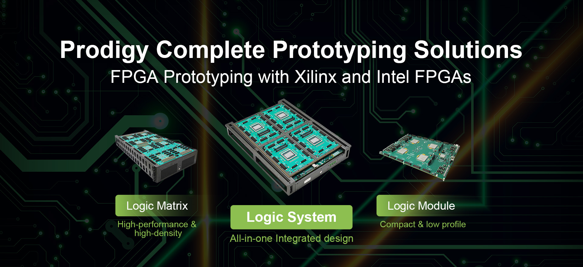
Confronted with these challenges, S2C Prototyping Solutions emerged as a trusted ally, offering a streamlined pathway for verification and demonstration, empowering developers to amplify the unique value propositions of their SoCs.
Automated Design Partitioning:
S2C offers a comprehensive suite of tools that facilitate and enhance design verification. The Prodigy PlayerPro, a highly automated solution engineered to perform intricate partitioning tasks using sophisticated algorithms without manual oversight, optimizes FPGA resource allocation and minimizes inter-FPGA signal latency. This significantly improves the success rates of FPGA placement and routing. Enhanced with FDC constraint-based partitioning and automated I/O assignment, PlayerPro efficiently streamlines the prototyping workflow, substantially reducing bring-up times and accelerating iterative development through ECO Flow.
Industry-leading Performance:
S2C’s Prodigy Prototyping Solution leverages advanced TDM Aware technology to optimize Time Division Multiplexing (TDM) ratios based on timing criticality, ensuring each system meets the highest performance benchmarks. This capability is augmented by system-level Static Timing Analysis (SSTA), which proactively identifies and mitigates potential performance bottlenecks early in the design phase, significantly boosting the efficiency and outcome of projects.
Robust and Stable Platform:
Engineered for high performance and uniformity, the S2C Prodigy Prototyping platform is underpinned by rigorous production process oversight, stringent quality control standards, and robust supply chain capabilities. This solid foundation guarantees dependable and consistent outcomes, crucial for the success of product development.
Comprehensive Solutions:
To address the diverse needs of the industry, S2C offers an extensive range of peripherals and reference designs. With over 90+ ready-to-use daughter cards, PCIe5 Speed Adapters, Memory DFI PHYs, and ChipLink IP solutions, S2C ensures that all aspects of system integration are covered, providing exceptional performance, and simplifying the entire design and verification process.
With over 20+ years of industry experience and a relentless commitment to innovation, S2C equips clients with highly trusted tools necessary to stay ahead in the competitive market. Our solutions accelerate the time-to-market successfully, delivering unparalleled speed, accuracy, and dependability.
For more information please visit: https://www.s2cinc.com/
Also Read:
Accelerate SoC Design: DIY, FPGA Boards & Commercial Prototyping Solutions (I)
S2C and Sirius Wireless Collaborate on Wi-Fi 7 RF IP Verification System
Enhancing the RISC-V Ecosystem with S2C Prototyping Solution
Share this post via:


Comments
There are no comments yet.
You must register or log in to view/post comments.