AI requires more Silicon capacity
Deep in the supply chain, some wizards turn sand into perfect diamond-structured crystal disks of silicon, which are necessary for the entire semiconductor supply chain.
They are part of the semiconductor supply chain, making Silicon Sand almost a thousand times more valuable.
![]()
The glimmer you see on the beach is Silicon. Silicon is a complex crystalline, brittle and solid metalloid (Metal and non-metal properties). Silicon is everywhere.
Behind oxygen, silicon is the 2nd most common material on Earth and the 7th most common material in the universe.
Silicon is a Semiconductor, which means it has electrical properties between a conductor (such as copper) and an insulator (such as glass).
A minute amount of foreign atoms in the silicon structure can radically change its behaviour, so semiconductor-grade silicon has to be incredibly pure. The lowest acceptable purity for electronic-grade silicon is 99.9999999%.
This means that only one non-silicon atom is allowed for every billion atoms.
Good drinking water allows for 4M non-water molecules, 500.000 times less pure than Semiconductor-Grade Silicon.
The blank wafer manufacturers must transform the High-Purity Silicon into a perfect Monocrystalline structure. This is done by introducing one single mother crystal into molten silicon at the right temperature. As new identical baby crystals start to grow around the mother crystal, the silicon ingot is slowly created out of the molten silicon.
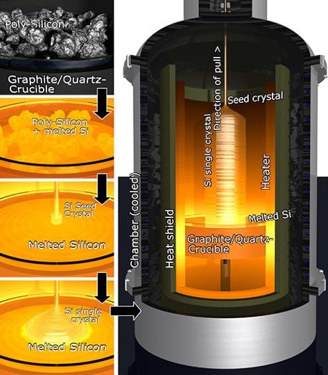
This process is slow and can take up to a week. The finished ingot weighs in at around 100 kg and can create over 3,000 wafers.
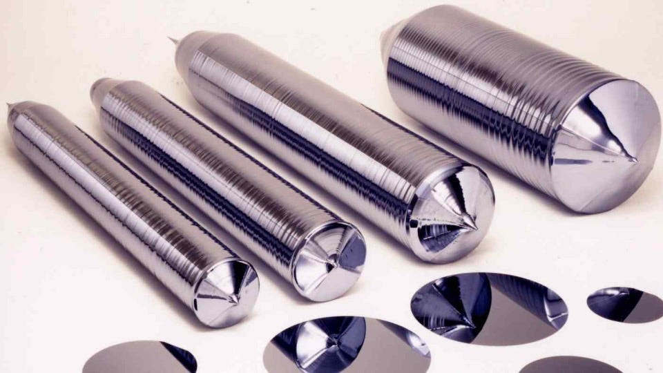
A very thin diamond wire saws the silicon ingots into wafers two hair widths in size. The silicon-cutting tools are highly accurate, and the operators must be under constant supervision, or they will start using the tools to do silly things to their hair.
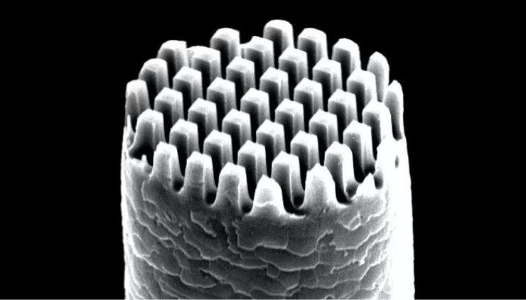
This simple walkthrough of manufacturing blank wafers is criminally simplified and does not give sufficient credit to the wizards; it hopefully has provided a background for the dive into the blank wafer business.
Supply and demand in blank wafers
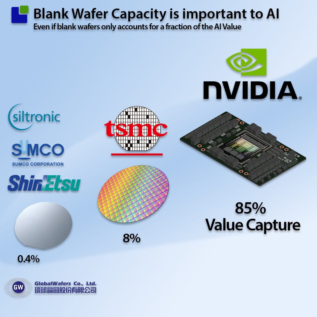
The blank wafer market is dominated by the four companies below. For long periods, the market has been in a delicate borderline capacity balance between supply and demand.
The dip in semiconductor sales in 2023 catapulted the market into oversupply, resulting in high internal and external inventories at chip manufacturers.
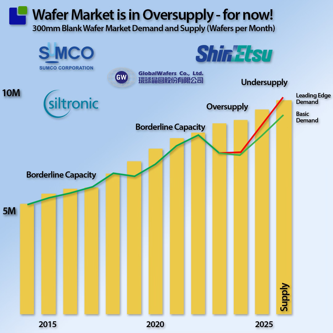
However, this is a temporary situation. As the market recovers, the industry will soon return to borderline capacity and must accommodate additional demand from the AI revolution.
The transformation from traditional CPU-based architectures to accelerated computing will impact the industry as it will require more silicon area than conventional architectures of the past.
Nvidia and TSMC will get the blank wafers they need, as the cost of the wafer compared to the total system cost is fractional. However, this could impact lower-value areas of the Semiconductor industry.
GPU architectures need more Silicon area.
As the hunger for performance increases, GPU manufacturers must battle several design limitations to extract more performance from their GPUs.
Making the die larger is an apparent way of getting higher performance, as electrons don’t like travelling long distances between different chips, which limits performance. However, there is a practical limit to how large it is possible to make the dies called the Reticle limit.
The reticle limit refers to the maximum size of a die that can be exposed in a single step on a photolithography machine used in semiconductor manufacturing. This limit is dictated by the maximum field size of the photolithography equipment, particularly the stepper or scanner used in the lithographic process. As of recent technology, the reticle limit is typically around 858 mm².
This size limitation is significant because it determines the maximum area that can be patterned on a wafer in one exposure. If a die is larger than this limit, multiple exposures would be required to fully pattern the die, which is impractical for high-volume manufacturing due to complexity and alignment challenges.
The new GB200 will overcome this limit by combining two reticle-limited dies on a silicon interposer, creating a super die 2x the reticle limit.
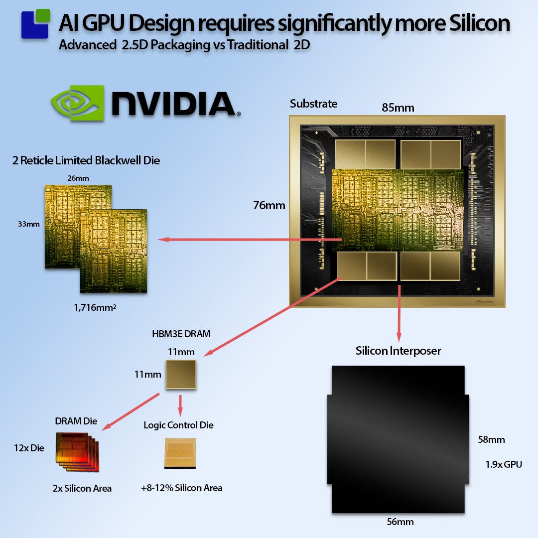
The other performance limitations are the amount of memory and the distance to it (translates into memory bandwidth). The new GPU architectures overcome this by using stacked High Bandwith Memory mounted on the same silicon interposer as the two GPU dies.
The problem with HBM from a silicon perspective is that the silicon area per bit is 2x traditional DRAM due to the highly parallel interface needed to create the high bandwidth. HBM also incorporated a logic control die in each stack, adding to the silicon area.
A rough calculation shows that a 2.5D GPU architecture uses 2.5x to 3x the silicon area that a traditional 2.0D architecture would use.
As was seen earlier, the blank wafer capacity will likely be very tight again unless the wafer companies are ready for this change.
The future capacity of the blank wafer market
The first of three laws of semiconductor manufacturing states that you need to invest the most when you have the least. This is due to the industry’s cyclical nature, which is very hard for semiconductor companies to follow.
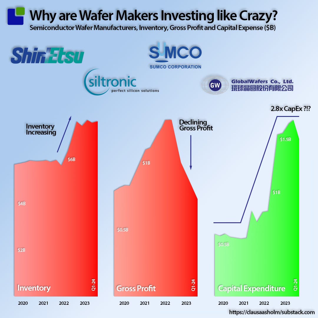
As can be seen below, most of the blank wafer manufacturers are aware of the impact of this change, and the combined quarterly Capex has ballooned by almost threefold over the last few quarters. This is despite the difficult market conditions faced by the blank wafer companies.
What is even more interesting is that this trend started a long time ago. The blank wafer companies got lucky or knew something others did not.
The Semiconductor supply chain is a Time Machine that can predict future things. Your future might be somebody else’s past. While we don’t always get answers, we almost always get questions worth interrogating.
Also Read:
What’s all the Noise in the AI Basement?
Tools for Chips and Dips an Overview of the Semiconductor Tools Market
Tools for Chips and Dips an Overview of the Semiconductor Tools Market
Share this post via:


Is Intel About to Take Flight?