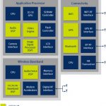
It seems only appropriate that at the beginning of the year we should look at who is going to be the next significant threat to Apple’s profitability machine. During Apple’s meteoric rise over the past 9 years (APPL share price: Jan-2004 @ $11 vs. Jan-2013 @ $550) different companies have been put up as Apple’s next significant threat… Read More


Are you good at identifying languages? Win an iPad Mini
Did you watch Atrenta’s holiday video (it’s only one minute)? Various Atrenta employees from all over the world wished you happy holidays in their own languages. Now Atrenta are having a competition. If you identify all the languages in the video then you can win an iPad Mini.
To enter the competition, or to view the … Read More
HiFi Mini, Always Listening
Next week it is the Consumer Electronics Show (CES) in Las Vegas and so there are announcements around the areas where consumer overlaps with semiconductor, which these days is primarily mobile. Then in February in Barcelona is Mobile World Congress, which is even more focused on mobile. Expect more announcementst there.
Currently… Read More
Integrating your SoC into the analog world
Our world is decidedly analog, made up of stimuli for our five basic senses of sight, touch, hearing, taste, and smell, and more advanced senses like balance and acceleration. To be effective on the Internet of Things, digital devices must integrate with the analog world, interfacing with sensors and control elements.… Read More
The Semiconductor Landscape – II
It has been a year since my article Semiconductor Landscape in Jan 2012 I wanted to look back into the major events over the year and then anticipate what’s in store going forward. What has happened over the year is much more than what I could foresee. Major consolidation in EDA space – Synopsys acquired Magma, SpringSoft, Ciranova,… Read More
Wafer Costs: Out of Control or Not?
I didn’t attend the International Electronic Device Meeting (IEDM) earlier this month, but there have been a lot of reports on the inter webs especially about 20nm and 14nm processes. Some of this is really geeky stuff but I think that perhaps the most interesting thing I’ve read about is summarized in this chart:
This… Read More
Happy New Year from SemiWiki!
It was an amazing year for SemiWiki and I would like to sincerely thank all who participated. SemiWiki traffic doubled again which is amazing in itself. SemiWiki membership more than tripled as we continue to add vertical markets (EDA, IP, Services, Foundry). More people are blogging on SemiWiki and the Forums and Wikis are coming… Read More
Phablet, e-reader, Nexus
In November and December I upgraded three devices and share my opinions on the utility of each:
- Samsung Galaxy Note (aka Phablet = Phone + Tablet)
- Kindle Paperwhite (e-reader)
- Google Nexus 7 (Tablet)
Cadence 3D Methodology
A couple of weeks ago was the 3D Architectures for Semiconductor Integration and Packagingconference in Redwood City. Cadence presented the changes that they have been making to their tool flow to enabled 2.5D (interposer-based) and true 3D TSV-based designs. You know what TSV stands for by now right? Through-silicon-via, … Read More
Intel 22nm SoC Process Exposed!
The biggest surprise embedded in the Intel 22nm SoC disclosure is that they still do NOT use Double Patterning which is a big fat hairy deal if you are serious about the SoC foundry business. The other NOT so surprising thing I noticed in reviewing the blogosphere response is that the industry term FinFET was dominant while the Intel… Read More
Facing the Quantum Nature of EUV Lithography