Atmel was founded in 1984. The name stands for “advanced technology for memory and logic” although initially the focus was on memory. George Perlegos the founder had worked in the memory group of Intel back when Intel was a memory company and not a microprocessor company although that didn’t stop Intel suing… Read More
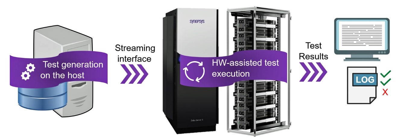 When Software Outruns Silicon: Hardware-Assisted Test Generation to the RescueFor the past decade, the semiconductor industry has…Read More
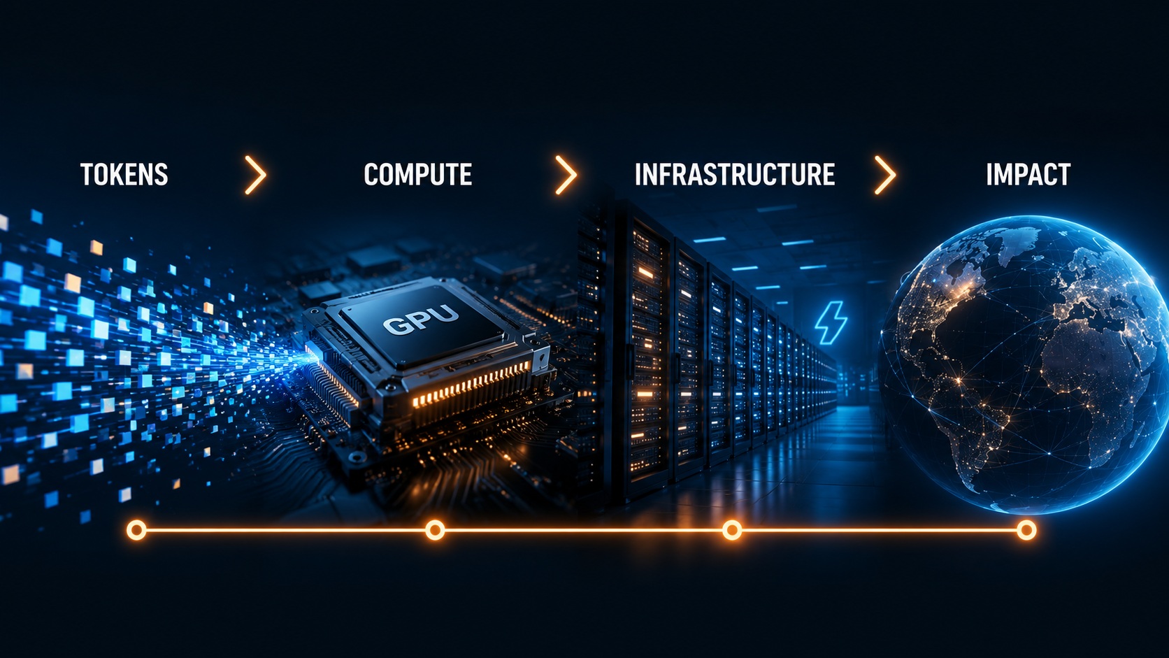 From Tokens to Infrastructure: Why Compute, Memory, and Power Will Determine the Future of AIBased on Dylan Patel’s SEMI Industry Strategy Symposium…Read More
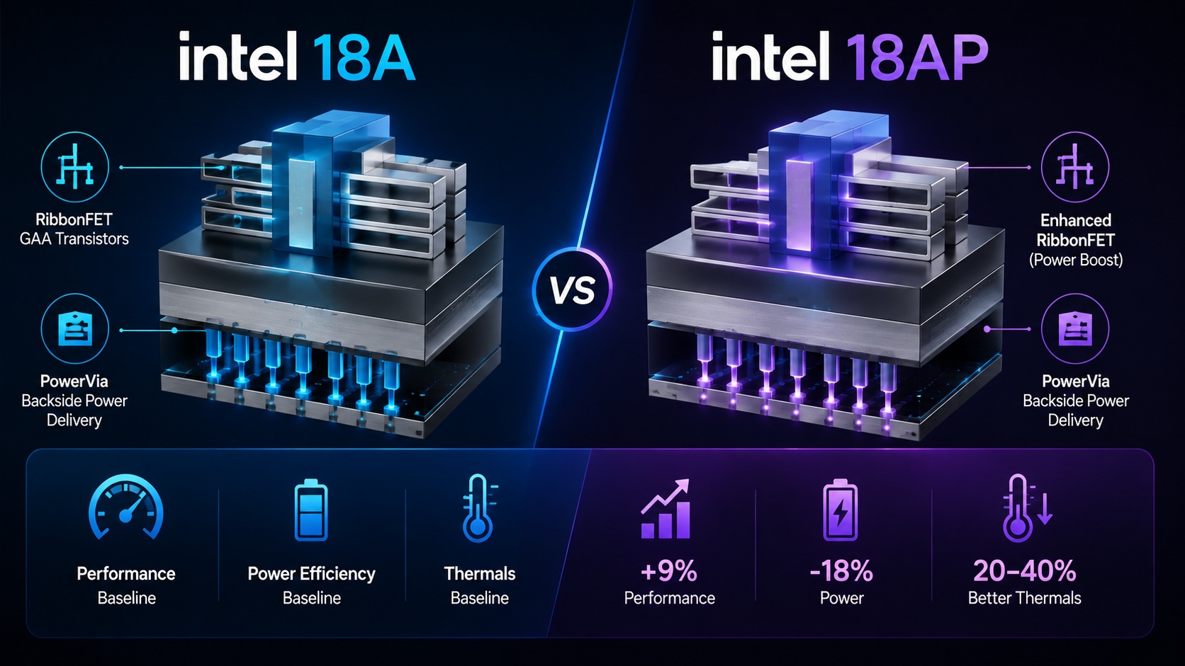 Intel 18A vs Intel 18A-P: What Is the Difference and Why Does It Matter?Intel’s 18A process technology has become one of…Read More
 WEBINAR: Why Google Cloud NetApp Volumes Matter for Modern EDA WorkloadsIn this webinar, Google Cloud and NetApp explore…Read More
 How to Free Yourself from Inconsistent Engineering Documentation Before It’s Too LateEmbedded systems programs often fail because critical engineering…Read More
ASTC and the new midrange ARM Mali-T720 GPU
When we last visited texture compression technology for OpenGL ES on mobile GPUs, we mentioned Squish image quality results in passing, but weren’t able to explore a key technology at the top of the results. With today’s introduction of the ARM Mali-T720 GPU IP, let’s look at the texture compression technology inside: Adaptive… Read More
ARM Announces A17
It is microprocessors all the time right now, with Linley last week. Today ARM announced the next generation Cortex-A17 core. It is a development built on the Cortex-A12 core, itself built on A7 (which is the current volume leader). ARM says that it is 60% faster than the A7 core, although I’m sure a lot of that gain is a process… Read More
If you still think that FDSOI is for low performance IC only…
…then you should read about this benchmark result showing how digital power varies with process corners, for high-speed data networking chip, not exactly the type of IC targeting mid-performance mobile application. Before discussing the benchmark results, we need to have some background about this kind of ASIC chip. Such a … Read More
Data Outgrowing Datacenter Performance
Last week I attended the Linley Datacenter Conference. This is not the conference on mobile which is not until April. However, a lot of the growth in datacenter is driven by mobile, with the increasing dominance of the model where data is accessed by smartphones but a lot of the backend computing and datastorage is in the cloud.
From… Read More
Update on AMS Verification at DVcon

Digital verification of SoCs is a well-understood topic and there’s a complete methodology to support it, along with many EDA vendor tools. On the AMS (Analog Mixed-Signal) side of the design world life is not so easy, mostly because there are no clear standards to follow.
To gain some clarity into AMS verification I spoke… Read More
TI – The Initial Innovator of Semiconductor ICs
[TI’s China Foundry acquired from SMIC]
During my engineering graduation, electronic design courses and mini-projects, the ICs I used to come across were SN 7400 series from Texas Instrumentsthat covered a large range of devices from basic gates and flip-flops to counters, registers, memories, ALUs, system controllers, and… Read More
Has LinkedIn Jumped the Shark?
LinkedIn is without a doubt the number one social network for semiconductor professionals. Based on my experience, the big LinkedIn boom came with the massive unemployment during the Great Recession of 2009. In my estimate, unemployment was 12%+ at the high point in Silicon Valley and resumes clogged the internet with LinkedIn… Read More
Who Won the DesignVision Awards at DesignCon this year?

The Seattle Seahawks had an awesome victory in the SuperBowl against the Denver Broncos, so folks living here in the Pacific Northwest are feeling proud and optimistic. The recent DesignConconference and exhibit ended 10 days ago and there were also victors announced in terms of the annual DesignVision awards that have three … Read More
What does a 52% increase in DSP IP core licensing means?
The future market performance for an IP vendor licensing an IP based on a model with upfront fee plus royalties can be easily and safely evaluated if you look at the first part of revenue: upfront fee. Even if the royalty part is declining, exhibiting a 52% increase (Q4 2013 to Q4 2012) in upfront licensing fee is a promise that the future… Read More
Why Huawei Says It Will Match TSMC’s Most Advanced Chips by 2031