Last night the IEEE Silicon Valley Chapter had a panel session that was in some ways a preview of some of what will be discussed at the Electronic Design Process Symposium in Monterey next Thursday and Friday. At EDPS Herb Reiter organized a session on FinFET, 3DIC and FD-SOI (sort of how many buzzwords can you get into one set of titles).… Read More
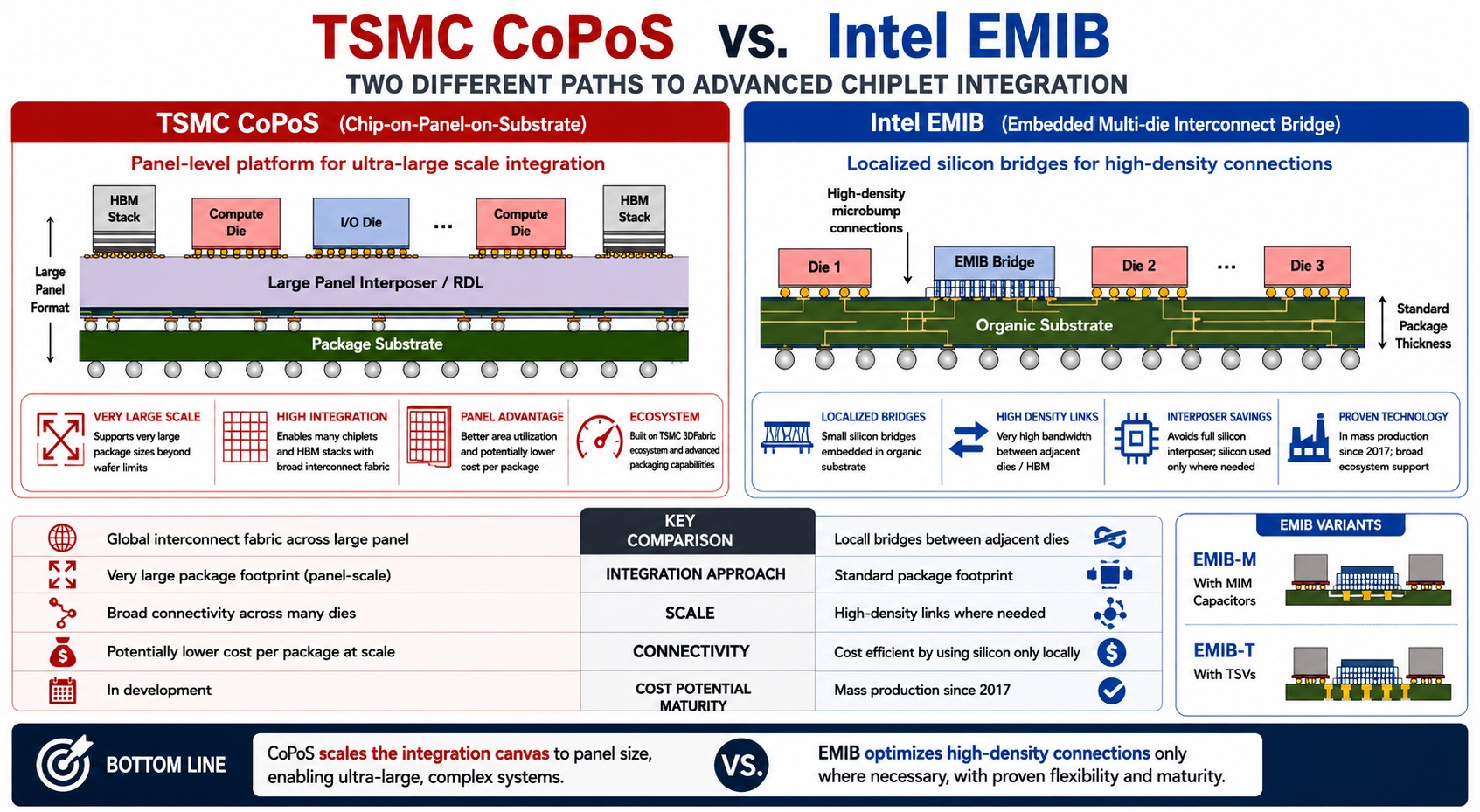 TSMC CoPoS Versus Intel EMIB Semiconductor PackagingTSMC’s CoPoS, generally described as Chip-on-Panel-on-Substrate, and Intel’s…Read More
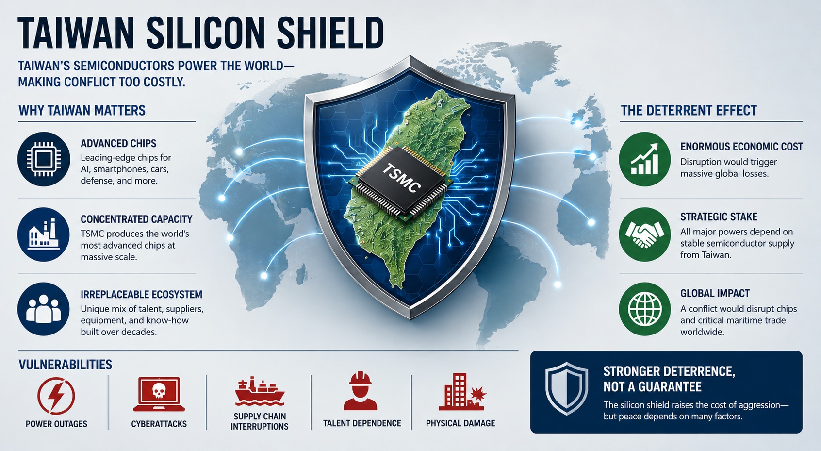 The Silicon Shield Has Never Been Stronger!The “Silicon Shield” describes the idea that Taiwan’s…Read More
 Agentrys Designs a Real Chip with its Multi-Agent WorkforceThe face of EDA is changing. For forty…Read More
 Must-See DAC Panel – Build vs Buy: Who Owns the Intelligence Behind Tomorrow's Chips?This year, DAC will be buzzing about AI…Read More
Addressing MCU Mixed Signal Design Challenges
The emerging market for IoT and wearable devices are designed with mixed-signal IP that includes: embedded CPU, flash, analogue and radio.EDA and IP companies have recently worked together to allow us to design an MCU with mixed-signal IP blocks more efficiently. This morning I attended a webinar with presenters from ARMand … Read More
How Qualcomm crushed the mobile roadmap
Qualcomm’s Snapdragon 810 announcement this week may seem like just another mondo-core SoC on a way-cool TSMC 20nm advanced process. Looking past the technology shows an understated genius in creating a roadmap – and why yours and most everyone else’s probably sucks.… Read More
IP Reuse and Management in Monterey!
One of the benefits of being part of SemiWiki is building relationships with a wide variety of companies covering every semiconductor design application imaginable. We are blessed, absolutely. Another benefit of being part of SemiWiki are the invitations to attend, participate, and even organize events such as EDPS. Last year… Read More
Who Wants to Live in Malta?
Who wants to live in Malta? A beautiful island in the eastern Mediterranean with wonderful food…wait, that’s the wrong Malta. I’m talking about the one in upstate New York where GlobalFoundries have their big fab 8 and also their technology development center (also known as fab 8.1).
So why would you want to … Read More
A New, Free, Web-Based EDA Toolset in the Cloud
In the 1990’s there was a push to build EDA frameworks, however they all failed because no user wanted to be locked into one EDA vendor tool flow. Fast forward to 2014 and there’s an emerging trend to use web-based EDA tools as a framework, instead of downloading and installing software to your desktop or device. I just… Read More
Sonics Performance Monitor and Hardware Trace
As SoCs have got more complex, and with a larger and larger software content, it is no longer good enough to just monitor how the design behaves using simulation and then completely forget about it once the design is complete. What is required is the capability to monitor the design in real time (in silicon or FPGA) to see how it is behaving.… Read More
A New Digital Place and Route System
IC place and route tools can be very high-priced EDA software to purchase or lease, so there’s some good news for AMS designers that need an affordable digital place and route tool for their mostly analog designs. Today the team at Tanner EDAannounced a totally new place and route system has been added to their Schematic Driven… Read More
SerDes: Four Wires Are Better Than Two
Kandou Bus SA has recently been proposing the technique ENRZ (Ensemble Non Return to Zero) for use as the next generation interconnect standard for the 56 Gb/s generation of interconnect interfaces at the OIF (Optical Interconnect Forum). ENRZ is technique where three bits are orthogonally modulated over four correlated wires.… Read More
Dinner with Dr. Walden C. Rhines!
You are cordially invited to have dinner with my favorite EDA CEO, Dr. Walden C. Rhines (the C stands for Clark by the way). Wally will be the dinner keynote speaker at the Electronic Design Process Symposium on April 17[SUP]th[/SUP] at the Yacht Club in Monterey. When registering use Promo Code: SemiWikiGofor $50 off. Such a deal!… Read More
Enhancing Multi-Domain System Simulation with FMI Co-Simulation