In his recent blog on EETimes, Kurt Shuler of Arteris took a whimsical look at the hype surrounding the IoT, questioning the overall absence of practicality and a seemingly misplaced focus on use cases at the expense of a coherent architecture. I don’t think it is all that bleak, but when it comes to architecture, Kurt is right, and… Read More
 The Accidental Infrastructure: How Crypto Miners Built the Foundation of the AI BoomMost crypto forty-niners died broke in a warehouse…Read More
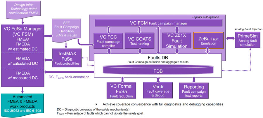 From Detection to Safety: Reframing Fault Simulation for Functional SafetyIn the early 1980s, when computer-aided engineering (CAE),…Read More
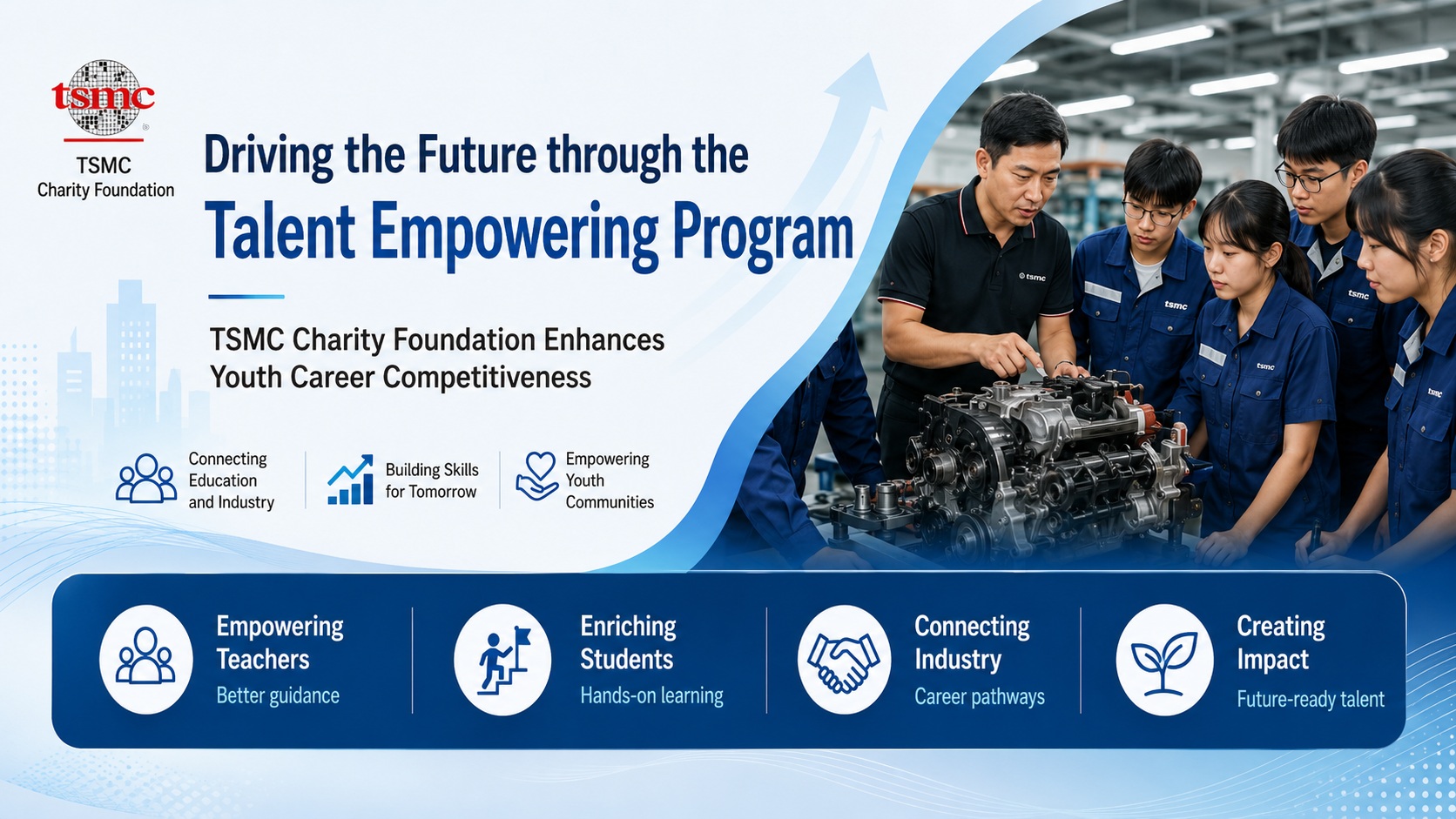 Driving the Future through the “Talent Empowering Program”: Why TSMC Charity Foundation’s Youth Career Initiative MattersThe future of work will not be shaped…Read More
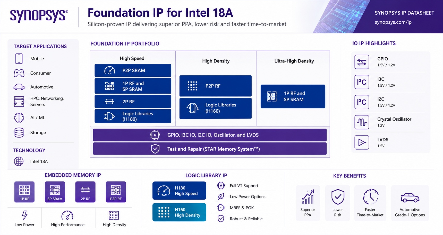 Foundation IP for Intel 18A: Technical Overview and Why It MattersSynopsys Foundation IP for Intel 18A is a…Read More
 WEBINAR: Defacto is Boosting Front-end SoC Design With AI-Powered EDA toolsThe real promise of AI in EDA is…Read More
Does Processor IP still get the Lion’s share in 2013?

I think that the answer is pretty obvious, but the interesting point is to figure out which processor type, and which part of revenues, up-front license or royalties? One of my customers, let’s call him Mr. X, ask me to clarify this point. Mr. X has bought the excellent report from Gartner “Market Share: Semiconductor Design Intellectual… Read More
Customization can add extraordinary power to your tool
In EDA arena we often find companies providing customization platforms along with the tools they offer to their customers. I admire such companies because they equip the end users of a tool to extend its functionality as they like according to their environment, thus increasing the designer productivity significantly. And I’m… Read More
Intel Lost $1B in Mobile Last Quarter
Intel announced their quarterly results today. Revenue was $12.8B, up 1% from a year ago with operating income of $2.5B also up 1% from last year.
Since the future of the world is mobile and not desktop/laptop, the mobile results are the most interesting. Mobile sales fell 61% to $156M. This includes mobile products and anything … Read More
Xilinx Showcases Worlds First ‘High Performance’ Analogue FPGA
Last February Xilinx presented a prototype device at the 2014 IEEE international Solid-State Circuits Conference (ISSCC, titled “A Heterogeneous 3D-IC Consisting of Two 28nm FPGA Die and 32 Reconfigurable High-Performance Data Converters” and click here to get a copy of the paper. Let me just share the intro my dear reader… … Read More
What, SD doesn’t have enough pins?
I was in a Twitter conversation over the weekend with some very smart people, and one of the discussion points was how slow and painful the formal standardization process can be. One suggestion was that IoT companies should “just do it”, creating specification-by-implementation. … Read More
Automobiles and DAC
On SemiWiki we have some 247 blogs and forum discussions on the topic of “automotive“, so I’m pleased to learn that at DAC in San Francisco there is a new track just for automotive systems and software. Just consider all of that electronic content in your typical auto:… Read More
Will IoT Drive the Next Semiconductor Revolution?

To further my quest to comprehend the latest trends in the semiconductor industry continues, I spent the morning with SEMI at the “The Silicon Valley Breakfast Forum: Internet of Things (IoT) – Driving the Microelectronics Revolution” seminar. I’m a big fan of the breakfast seminar concept. I’m up early anyway and it is … Read More
Show Me How To Get Better DRC and LVS Results For My SoC Design

Most IC engineers learn best by hands-on experience when another more experienced person can show us what to do. If you cannot find that experienced person, then the next best thing is a video from an expert. I was surprised to find out that video was so important today that the #2 most viewed web site on the Internet was www.youtube.com… Read More
Fast & Accurate Thermal Analysis of 3D-ICs
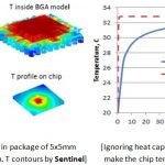
As Moore’s law started saturating on a single semiconductor die, the semiconductor community came up with the approach of growing vertically by stacking dies one above other in a 3D-IC arrangement. However, a major concern with a 3D-IC is that the heat generated by each die can get trapped in the stack, and hence it’s extremely important… Read More
Consolidation and Competition: Who is Winning the $4.5 Billion Interface IP Race?