One of the strengths of the fabless semiconductor ecosystem is competition since it keeps innovation high and prices low. One of the challenges of fostering competition is that you have to make good on a threat of using a competing product during a pricing negotiation. Well, in my opinion, for the next version of the iPhone, Apple… Read More
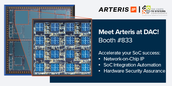 Arteris at DAC 2026 Connecting Innovation for Silicon SuccessThe semiconductor industry has entered a new era…Read More
 DAC 2026 Mach42: A new generation of physics-driven AI models for analog circuit verificationMach42 spun out of the Department of Physics…Read More
 Synopsys at Design Automation Conference 2026Synopsys is catalyzing the era of pervasive intelligence…Read More
 DAC 2026: Join Accellera for a dynamic luncheon exploring how artificial intelligence is reshaping the standards landscape for design and verification.Accellera Systems Initiative invites the design and verification…Read More
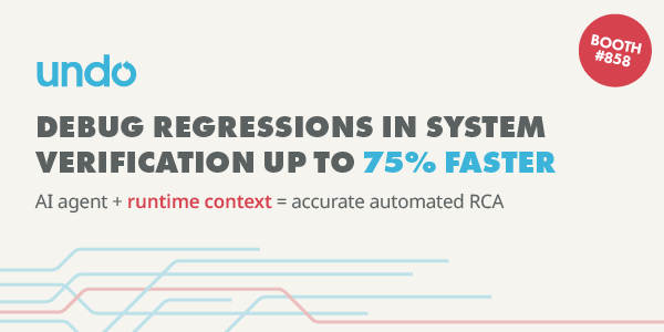 Enabling AI to Understand Complex Runtime Behavior for Accurate, Automated Root Cause Analysis — DAC 2026Undo gives AI coding agents the runtime context…Read More
Key Collaboration to Enable Designs at Advanced Nodes
In the semiconductor ecosystem, several partners (or better to say stakeholders) join together in the overall value chain to finally output the most coveted chip, err I should say SoC these days. It becomes really interesting when we start analyzing the real value added by each of them, none appears to be less. Well, then to whom … Read More
GlobalFoundries and Samsung at ARM
It was back in April that GlobalFoundries and Samsung announced that GF would license Samsung’s 14nm process to run in their Fab8 in upstate New York. Since then there has not really been any news and of course those of us that follow the foundry industry wondered to what extent there was real substance to the agreement or if … Read More
A de-parallel universe for Windows 10
It was CES 2011 when Steve Ballmer sweatered up and pitched the coming universe according to Microsoft, where the same Windows base would run on everything – PC, phone, tablet, and game console. Getting from that visionary statement to Windows 10 hasn’t been a smooth ride.… Read More
ARM ♥ TSMC!
This week is the 10[SUP]th[/SUP] annual ARM Technical Conference in Silicon Valley. In regards to size, content, and relevance, I believe ARM TechCon is the #1 event for the fabless semiconductor ecosystem for sure. I attended keynotes, sessions, and walked the hallways on Wednesday and Thursday. I wish I could write about everything… Read More
What’s Behind Carbon System Exchange – How Will it Scale?
Earlier this year, when I was looking at Carbon’spast year performance which provided record breaking revenue with whopping jump in bookings, one thing was certain that Carbon Performance Analysis Kits (CPAKs) would drive major growth in future, not only for Carbon, but also for the semiconductor industry. It will initiate … Read More
Agile IC Development
If you have been involved in software development you have probably heard of the “waterfall” development methodology. This is the approach whereby a complete specification of the software is developed before a single line of code is written. Nowadays, few people develop software that way since it is too slow. And… Read More
Semiconductor double digit growth in 2014 & 2015
The global semiconductor market was US$82.2 billion in the second quarter of 2014 according to World Semiconductor Trade Statistics (WSTS). 2Q 2014 was up 4.8% from 1Q 2014 up 10.1% from 2Q 2013. Healthy growth should continue into 3Q 2014. The table below shows initial revenue growth guidance for 2Q 2014, final reported revenue… Read More
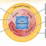
IP and Design Management Done Right
At DACin San Francisco this past June I was able to visit and blog about two dozen EDA companies, however there were so many more products and events to see that I couldn’t possibly have enough time to enjoy them all. Fortunately for me there were plenty of videos made of vendor presentations, so this week I got caught up a bit by… Read More
ANSYS Tools Shine at FinFET Nodes!
In the modern semiconductor ecosystem we are seeing rapid advancement in technology breaking past once perceived limits; 28nm, 20nm, 16-14nm, 10nm and we are foreseeing 7nm now. Double and multi-patterning are already being seen along with complex FinFET structures in transistors to gain the ultimate advantages in PPA from… Read More
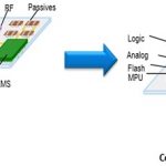
TSMC CoWoS versus Intel EMIB Semiconductor Packaging