Monday, January 4, 2016, Las Vegas, Nevada
Today I attended CES Unveiled, which offers a sneak peak at some of the new products being introduced at International CES 2016. The Internet of Things (IoT) has been hyped as a key driver of electronics market growth over the next few years. There were plenty of examples at CES Unveiled. … Read More
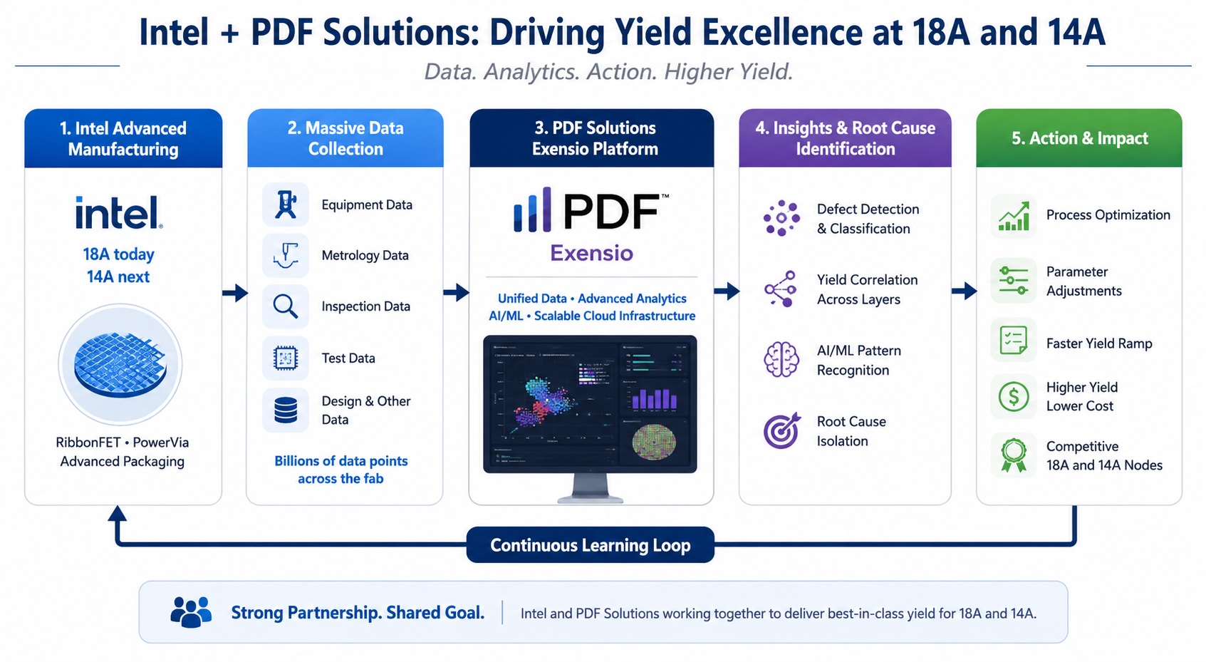 The Yield Partnership: Intel and PDF Solutions Tackle Advanced NodesOne of the most difficult things to do…Read More
 Webinar: Faster Design Spec to Implementation using IP-XACTAs SoC design flows grow increasingly complex, IP-XACT…Read More
 Webinar: Caspia Shows You How to Fix Security Flaws Before It’s Too LateI recently posted an overview of an upcoming…Read More
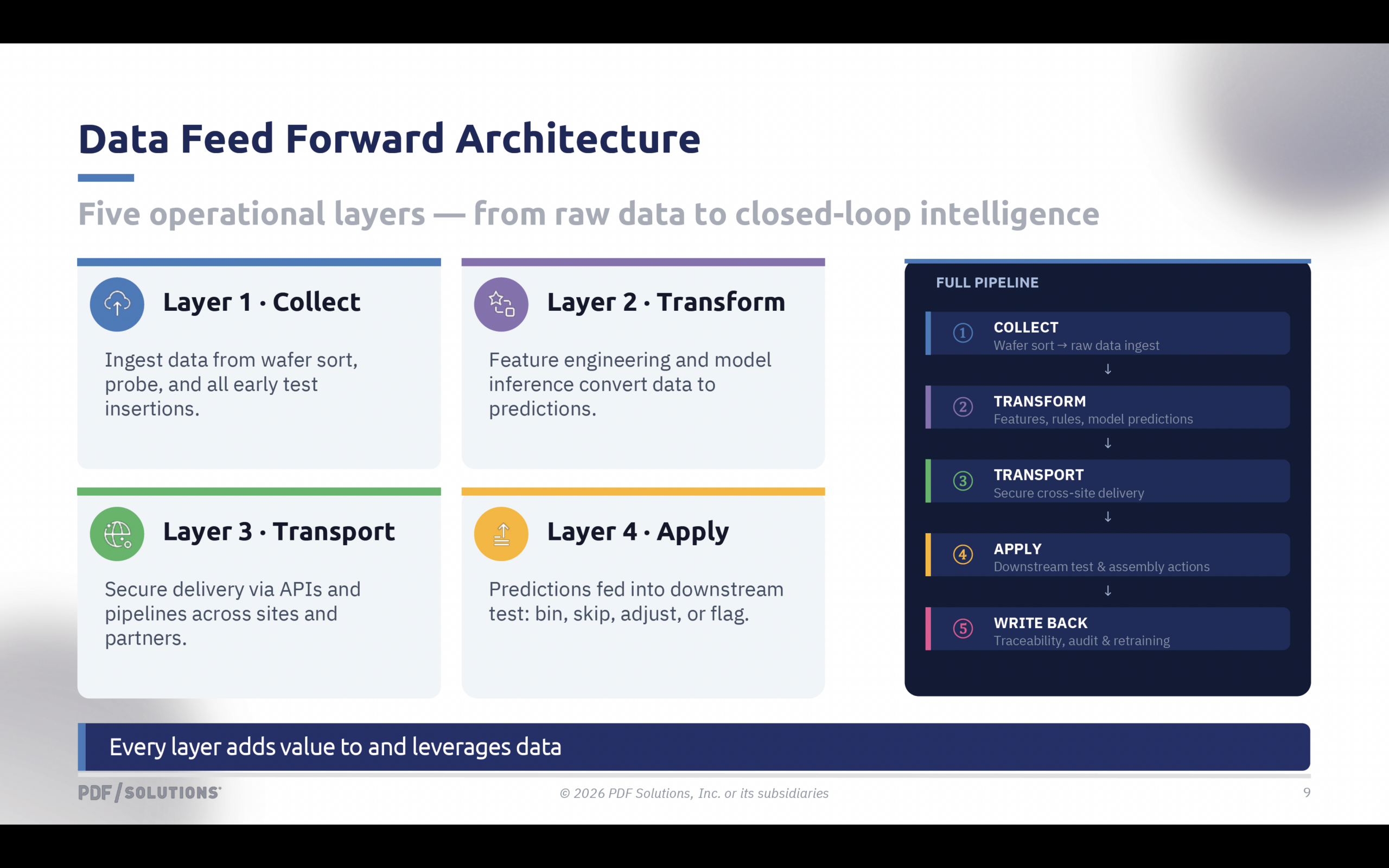 Feed Forward Intelligence: Enabling Testability in the Chiplets EraThe semiconductor industry is entering a new era…Read More
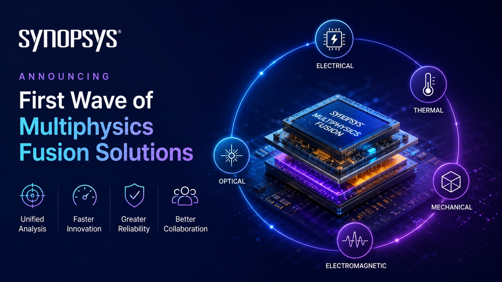 Synopsys Unifies Electrical, Thermal, Mechanical, and Optical Analysis with Multiphysics Fusion Solutions Market Leaders Including Cisco,…Read More
A System Spin on IoT Security
A lot of progress has been made in infrastructure to secure edge nodes in the IoT and to secure communications between edge nodes and gateways, all of which is good and necessary to block manifest evil, but it’s never enough. Perfect security is and always will be an asymptotic goal, so there should always be room for new ideas. To a … Read More
My Life at Fairchild – 1980-1983
After spending my first year learning a great deal about Diffusion and completing my orientation at Fairchild, I was moved to the 3″ Photolithography area as a sustaining engineer. As with the Diffusion area, being a sustaining engineer in Photo meant dispositioning lots on hold and making process improvements as needed.… Read More
Inventor of Netscape Looks at IoT
1995 was the year that a co-worker walked into my cubicle and said, “Hey, you have to see this new web browser and Internet thing.” I promptly installed Mosaic, later renamed Netscape, and began surfing the web with all of those interesting hyperlinks bringing me to new articles. Marc Andreessen was the mastermind … Read More
Who Does Voice Recognition in the Samsung Gear S2?
If you have bought a Samsung Gear S2 smartwatch for Christmas, you certainly didn’t open it to do a teardown. Chipworks did it and have shared the results: Qualcomm is the big winner here with five different chips: Snapdragon 400 as the main CPU of the system, the RF transceiver, the audio codec, the power and the baseband processor… Read More
Internet of Things 2015 Year End Review: IoT Business Ecosystem
Goldman Sachs defines the Internet of Things (IoT) as the third wave of internet revolution: By connecting billions of devices to the internet, the IoT can open up a host of new business opportunities and challenges. According to McKinsey, the IoT has the potential to create up to $6 trillion economic value annually by 2025. According… Read More
Semiconductors Future Hinges on a Single Pillar
A unique phenomenon has started manifesting itself under the slew of mergers and acquisitions this year in the semiconductor landscape. This phenomenon is bound to intensify in the near future and would positions itself as a key factor for the future of the semiconductor industry. The winners and losers in the game would be determined… Read More
2015’s Unfinished Automotive Business
The farther we come, the farther we have to go. While progress in advancing personal transportation was made in 2015, the year closes with glaring elements of unfinished business threatening to impede further progress toward mitigating highway fatalities and reducing emissions and congestion. These areas of unfinished business… Read More
The “Era of the Photon” is here!

The 50 year anniversary of the publication of Moore’s Law was recently celebrated, highlighting the tremendous advances in the Microelectronics Eraof the period in human history known as the Information Age. However, the technical and economic challenges currently faced by the microelectronics industry are bringing into… Read More
MediaTek X20 Benchmark Leaks: A Prelude to 2016 Mobile Chipset Wars?
MediaTek is making waves, again. The company’s flagship mobile system-on-chip (SoC)—Helio X20—is up against rivals like Apple, Qualcomm and Samsung, according to leaked Geekbench scores, and is leading in some of the performance benchmarks.… Read More
Available Is Not In Control: Balancing Output, Quality, and Risk in High-Volume Fabs