


In this era of high-performance, low-power, and low-cost devices coming up at an unprecedented scale, the SoCs can never attain the ultimate in performance; always there is scope for improvement. Several methods including innovative technology, multi-processor architecture, memory, data traffic management for low latency,… Read More
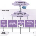
Advances in DDR IP Solution for High-Performance SoCs


Silicon Insurance: Why eFPGA is Cheaper Than a Respin — and Why It Matters in the Intel 18A Era