In March 2010 Efficient Power Conversion (EPC) proudly launched our GaN technology at the CIPS conference in Nuremberg, Germany. Parts and development kits were readily available off-the shelf and therefore designers could immediately get started with a new state-of-the-art semiconductor technology.
… Read More
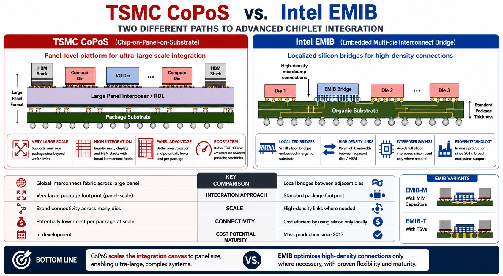 TSMC CoPoS Versus Intel EMIB Semiconductor PackagingTSMC’s CoPoS, generally described as Chip-on-Panel-on-Substrate, and Intel’s…Read More
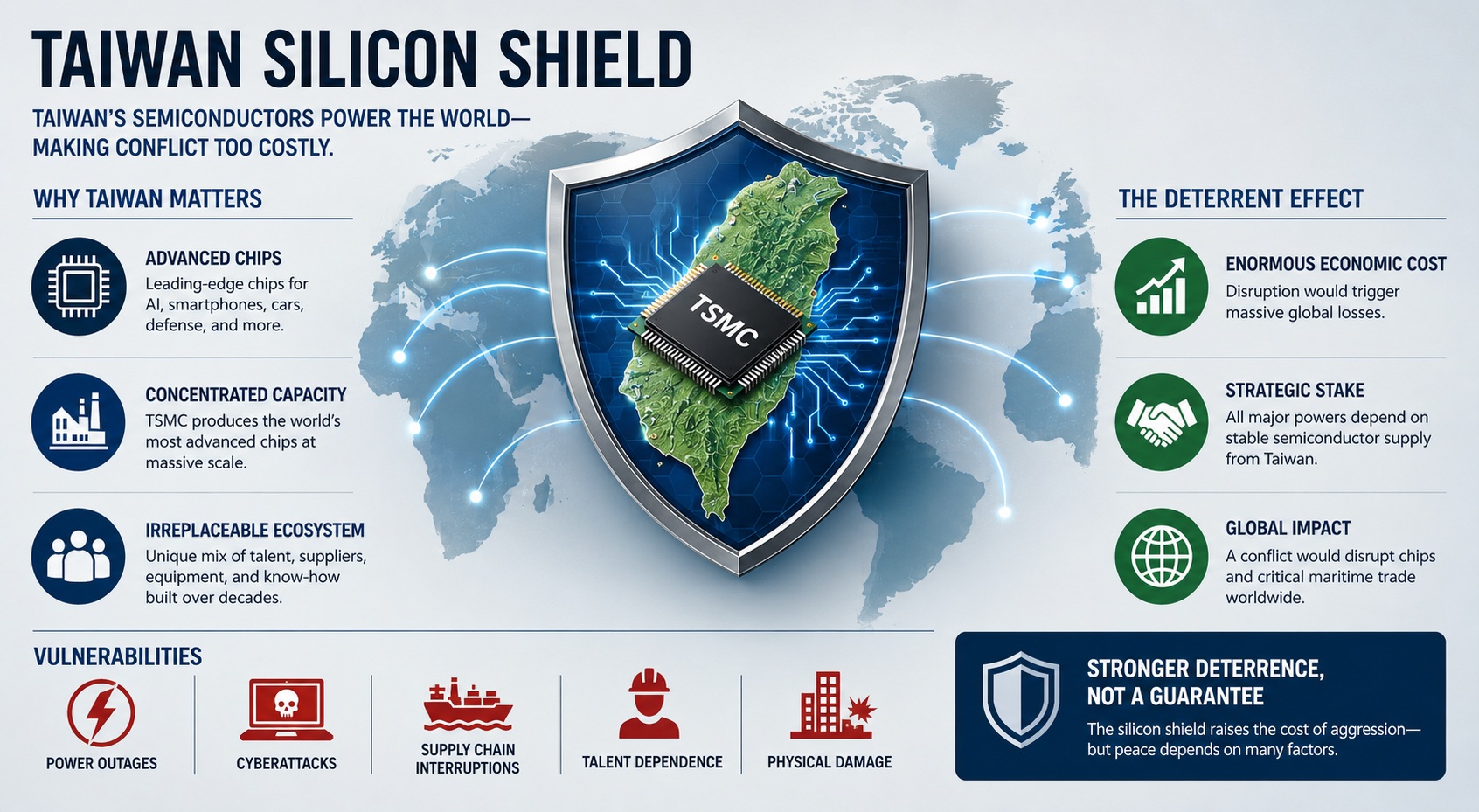 The Silicon Shield Has Never Been Stronger!The “Silicon Shield” describes the idea that Taiwan’s…Read More
 Agentrys Designs a Real Chip with its Multi-Agent WorkforceThe face of EDA is changing. For forty…Read More
 Must-See DAC Panel – Build vs Buy: Who Owns the Intelligence Behind Tomorrow's Chips?This year, DAC will be buzzing about AI…Read More
The Guiding Light & Other Photonic Soaps
I’m a child of the sixties and seventies and on the occasion when I was sick and couldn’t go to school I got to experience the world of daytime TV soap-operas. Back then we only got 3 channels and it wasn’t until the late 60’s that we got color TV! I remember titles like “The Guiding Light”, “Secret Storm”, and “As The World Turns”. Forty… Read More
OpenPOWER Keeps On Truckin’ At Annual Development Summit
The OpenPOWER Foundation, a collection of companies that have coalesced around IBM’s POWER architecture recently had their OpenPOWER Summit in San Jose, California. OpenPOWER was founded by IBM, Google, Tyan and Mellanox to coalesce around IBM’s approach towards opening up the POWER architecture to anyone that wishes to license… Read More
The chilling effect Peter Thiel’s battle with Gawker could have on Silicon Valley journalism
Gawker infringes on privacy and publishes tabloid-like stories that damage reputations. It is one of the most sensationalist and objectionable media outlets in the country. It also has not been kind to me. So it’s not a company that I would expect to be defending. But I worry that the battle that billionaire Peter Thiel has clandestinely… Read More
Intel’s New Strategy Is The Right One For The Company
Intel has been the focus of a lot of attention in the last week due to the company’s major restructuring announcement which came on the heels of Intel’s most recent earnings announcement. The majority of analyses that immediately followed the company’s announcement focused singularly on the layoffs, which amount to 11% of the … Read More
Highlights of the 28nm FD-SOI San Jose Presentations
Most of the presentations from the FD-SOI Symposium in San Jose last month (April 2016) are now available on the SOI Consortium website (click here to see the full list — if they’re posted, you can download them freely from there). If you don’t have time to wade through them all, here are some of the highlights. … Read More
Facebook and Deep Reasoning with Memory
Neural nets as described in many recent articles are very capable at recognizing objects and written and spoken text. But like anything we can build, or even imagine, they have limitations. One problem is that after training, the neural nets we usually encounter are essentially stateless. They can recognize static patterns but… Read More
Electrostatic Discharge analysis of FinFET technology
Sofics recently had the opportunity to characterize FinFET technology through cooperation with one of its customers. We analyzed the technology related to ESD and identified several challenges.… Read More
Free Webinar: Designing Low-Power IoT Systems

As I have written before, IoT looks to be a key driver for design starts and future semiconductor revenue growth which is why we wrote “PROTOTYPICAL” and included a field guide to FPGA Prototyping. If you want to get funding for your new IoT chip project, having a working prototype is a good thing, absolutely. If you want to take a look… Read More
My #53DAC Must See List!
It may be hard to believe but this happens to be my thirty third Design Automation Conference. Where does the time go? Three of my kids are out of college and the last one is getting close. That is where my time has gone. The conference itself started in 1964 but my first one was in 1984 in Albuquerque, New Mexico. In fact, that was the year… Read More
Enhancing Multi-Domain System Simulation with FMI Co-Simulation