Magwel CEO Dündar Dumlugöl is well known from his days at Cadence, where I first met him, and for his more recent tenure at Magwel. At Cadence he led the team that first developed Spectre. He has come a long way from the start of his career at IMEC in Belgium. He and I had a chance to have a conversation recently where he offered insights … Read More
 Siemens Wins Best in Show Award at Chiplet Summit and Targets Broad 3D IC Design EnablementThe recent Chiplet Summit in Santa Clara was…Read More
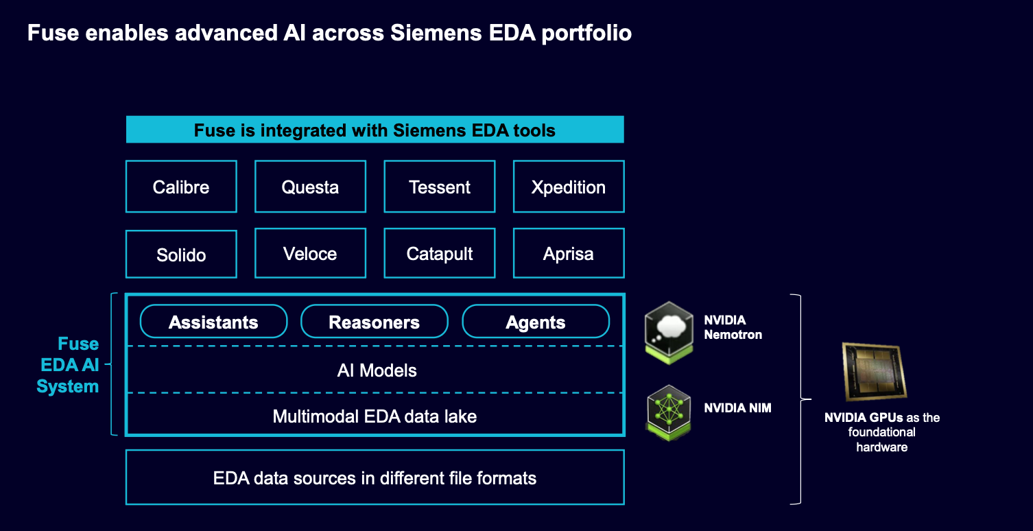 Siemens Fuse EDA AI Agent Releases to Orchestrate Agentic Semiconductor and PCB DesignThough terminology sometimes get fuzzy, consensus holds that…Read More
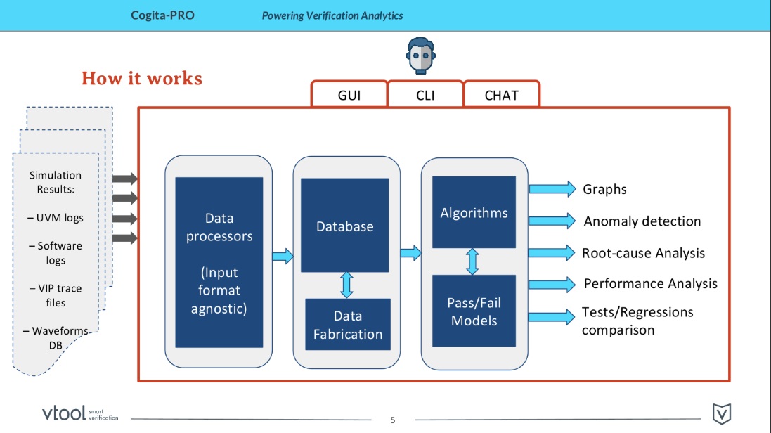 Verification Analytics: The New Paradigm with Cogita-PRO at DVCON 2026Cogita-PRO, developed by Vtool, introduces a transformative approach…Read More
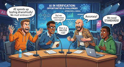 Breker Hosts an Energetic Panel on Spec-Driven VerificationI was fortunate to be asked to moderate…Read More
Building a Solar Powered Ice Freezer
My vacation is your worst nightmare. Well, at least that is what the bumper sticker says – it’s referring to Burning Man. It’s well known that among the tens of thousands of people attending this arts festival in Nevada at the end of each Summer there are lots of high tech luminaries. I also have gone many times – not to say that I am a luminary.… Read More
Top IOT News for 2016
2016 will go down as being part of the golden era for the Internet of things. This last year has experienced incredible advancements like cars that drive themselves, and cities that actually smarter. It has also been a learning experience where major security breaches threatened us, but we worked past them, and ultimately built… Read More
Mind-Boggling Uber Hubris
Uber was on a mighty roll throughout 2016 picking up strategic alliances with Ford Motor Company and Volvo Cars (for test vehicles) adding talent (cybersecurity experts Chris Vlasek and Charlie Miller) and acquisitions (Otto) and rubbing up against university researchers (Carnegie Mellon). So it was jaw-droppingly hideous… Read More
IEDM 2016 – 7nm Shootout
In the first session of IEDM on Monday, December 5th there were two papers presented on 7nm processes. The first paper was from TSMC and the second paper was from the Global Alliance of GLOBALFOUNDRIES, IBM and Samsung.… Read More
IEDM 2016 – GLOBALFOUNDRIES 22FDX Update
At IEDM in 2015 I had a chance to sit down with Subramani (Subi) Kengeri and get a briefing on GLOBALFOUNDRIES 22FDX technology. At IEDM 2016 Rick Carter of GLOBALFOUNDRIES presented a paper on 22FDX. Following Rick’s presentation, I had a chance to sit down with Rick and John Pellerin, VP of Technology and Integration and … Read More
Reducing the Cost of SoC Testing
Every year certain technology themes appear, like at ITC this year a big theme was how to reduce the cost of SoC testing. I spoke with Rob Knoth of Cadence by phone to hear more about this cost of test theme. Rob gave me an example of an SoC that takes 27 seconds on a tester, so at $0.04 per second in test costs amounts to $1.08 per part. If you… Read More
Enter the Cellular IoT
You could be forgiven for thinking that wireless in an IoT device must be Bluetooth-5 or Zigbee or Thread. After all, that’s what ARM has introduced as a part of their IoT solution and they have market weight that is difficult to dismiss. However those options aren’t the only game in town. There is already some level of (second… Read More
What Stephen Hawking gets right and wrong about the most dangerous time for our planet
Stephen Hawking made a bold headline last week: “This is the most dangerous time for our planet.”
In an essay in the Guardian, the renowned theoretical physicist wrote: “Whatever we might think about the decision by the British electorate to reject membership of the European Union and by the American public to embrace Donald Trump… Read More
Cybercriminals Next Targets: Long Term Prizes (part 2 of 2)
In the previous blog, Cybercriminals Next Targets: Short Term Dangers (part 1 of 2), I outlined how cybercriminals will use the holiday season to victimize unwary consumers and target businesses. They will also dive deeper into leveraging Internet-of-Things (IoT) devices. The longer-term outlook expands their reach to more… Read More


Captain America: Can Elon Musk Save America’s Chip Manufacturing Industry?