You are currently viewing SemiWiki as a guest which gives you limited access to the site. To view blog comments and experience other SemiWiki features you must be a registered member. Registration is fast, simple, and absolutely free so please,
join our community today!
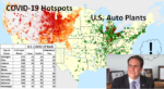
General Motors President Mark Reuss told Reuters last week that he is worried about the COVID-19 pandemic currently running rampant in the U.S. and globally. “I’m so worried about it because it’s accelerating and it’s not being contained,” he said during a “fireside chat” at the Reuters Automotive Summit which concludes Monday.… Read More
If you search on “the six signs” you will find references to a fantasy novel, “The Dark is Rising Sequence” by Susan Cooper. In this fantasy work there are six signs: wood, bronze, iron, water, fire and stone. Their purpose has something to do with driving away the Dark. Here is a quote from the book that puts these six signs in some context:… Read More
Back in July I first read the news that Perforce had acquired Methodics, and wasn’t too surprised, because many of the EDA vendors that we blog about do get acquired or merge with similar sized companies in order to be part of a bigger offering. When Methodics announced a webinar introducing IPLM 3.0 (IP Lifecycle Management),… Read More
I’ve become a bit of a connoisseur of voice-based control, so when Chris Rowen did a pitch on Babble Labs at Arm Dev Summit last month, I wanted to listen in. Chris was the CEO of Babble Labs, recently acquired by the Cisco Webex group where he’s now listed as VP Engineering of the Voice Technology Group. You should expect to see this… Read More
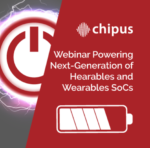
Chipus is an interesting company. It’s been around since 2008 and focuses on mixed-signal ASICs, intellectual property blocks and IC design services. They are headquartered on the island of Florianopolis, which is described as the most dense startup ecosystem in Brazil. The company has substantial skills in analog and mixed… Read More
Well, it’s official, the TSMC Board of Directors approved an investment to establish a wholly-owned subsidiary in Arizona with a paid-in capital of $3.5 billion. As history shows the investment may be more than that but $3.5B is a great starting point. This is being discussed in the SemiWiki Forum and I have been gathering inside… Read More
2020 has been a NAND growth year-2021 will be the year of DRAM. While foundry logic has gotten all the credit in 2020 the reality is that NAND has been up 2X in 2020 for semiconductor equipment provider Applied Materials (AMAT). It is expected that NAND will be flat in 2021 while DRAM will take over the growth slot with foundry/logic … Read More
Power seems to be on everyone’s mind these days. Hyperscale data centers worry about operating costs unless power is optimized. The AI accelerators in the Edge can’t be effective without optimized power. Advanced 2.5 and 3D packages simply can’t remove the heat unless power is optimized. And then there’s all those gadgets we … Read More
“For more than 18 years, we never stopped innovating at Defacto. We are aware of EDA Mantra “Innovate or Die!”. Innovation is in our DNA, and we never stopped adding new automated capabilities to the SoC design community to help facing complexity and cost challenges, which increase every year.”
Before founding Defacto… Read More
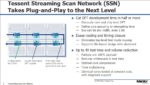
Design for test (DFT) requires a lot of up-front planning that can be difficult to alter if testing needs or performance differ from initial expectations. Hierarchical methodologies help in many ways including making it easier to reduce on chip resources such as the number of test signals. Also, hierarchical test allows for speed-ups… Read More


TSMC CoWoS versus Intel EMIB Semiconductor Packaging