



Dr. Talluri joined K&S in August 2026 as a member of the Board and assumed the role of President and Chief Executive Officer of K&S in September 2026. Prior to joining K&S, Dr. Talluri served as President, Chief Executive Officer and a member of the Board of Directors at Enovix Corporation, a Nasdaq-listed advanced … Read More
The Industry Challenge: AI Is Forcing Semiconductor Innovation Beyond the ChipApplied Materials President and CEO Gary Dickerson with…Read More
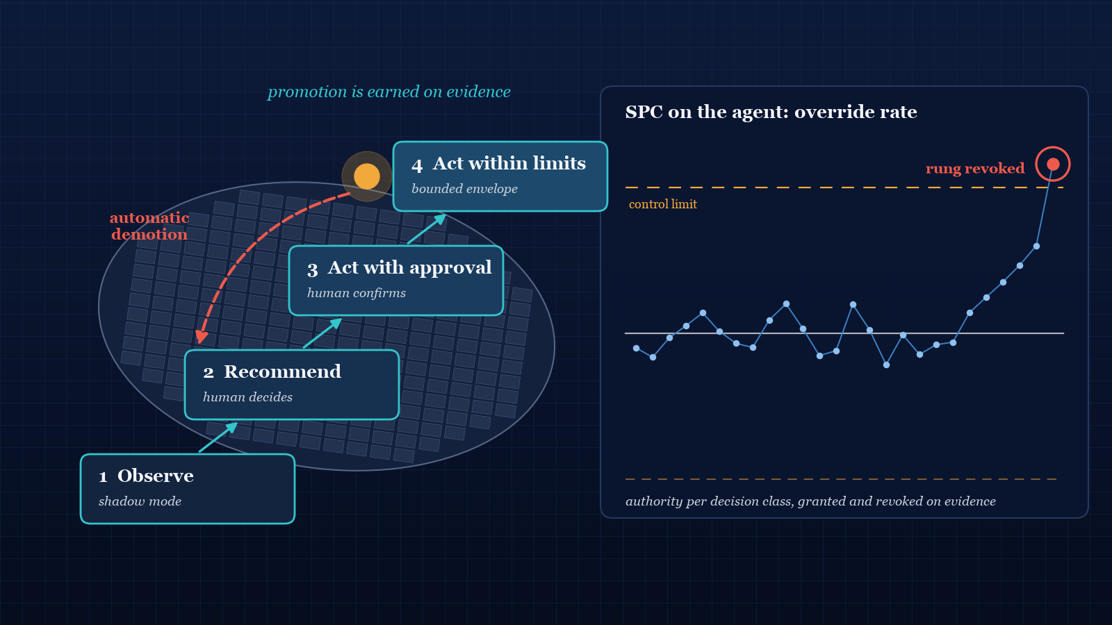
Who Gets to Move the Recipe? How Autonomous Agents Earn Decision Authority in the Fab Autonomy is granted per…Read More
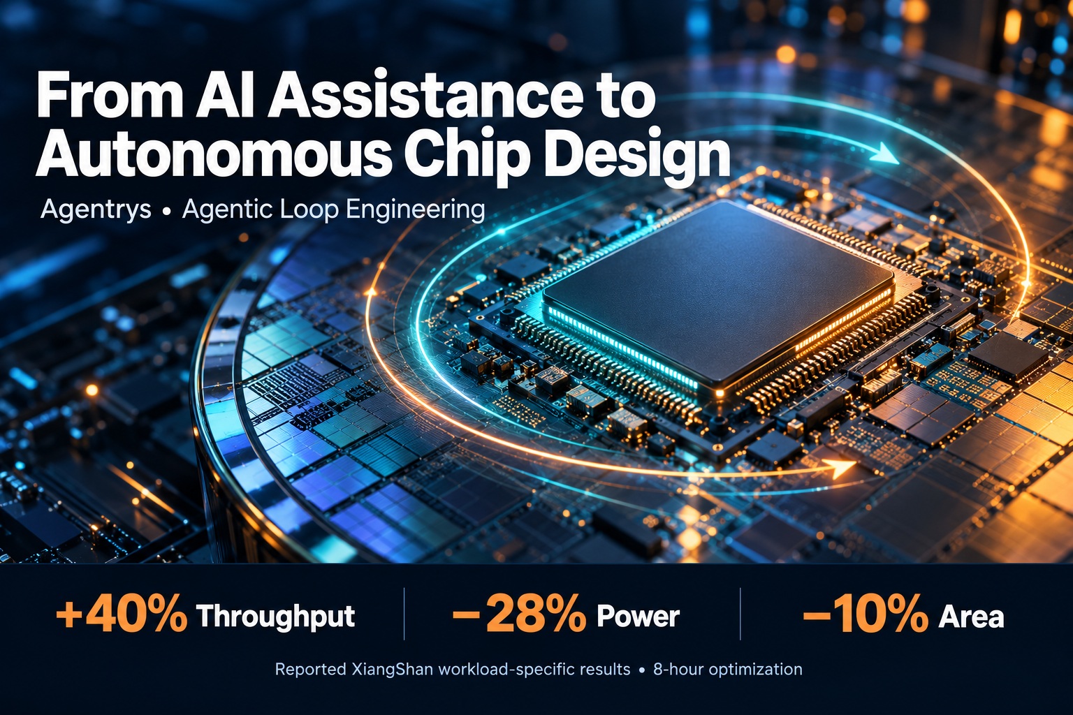
Moving Beyond AI-Assisted Design – Agentrys Shows the Way with Agentic Loop EngineeringAt Hot Chips 2026, OpenAI presented Jalapeño, an…Read More
Rethinking Phase Jitter: An Algorithmic Approach to Signal IntegrityByline: Richard Shreiner Modern semiconductor architectures are pushing…Read MorePodcast EP374: How proteanTecs Tames Multi-Die Packaging Challenges with Nir Server
Daniel is joined by Nir Sever, an industry veteran with over 30 years of technological and managerial experience in advanced VLSI engineering. Before joining proteanTecs, Nir served for 10 years as the COO of Tehuti Networks, a pioneer in the area of high-speed networking Semiconductors. Prior to that, he served for 9 years as … Read More
TSMC’s AI Expansion Signals a Broader Shift in Computing
TSMC is describing an artificial intelligence boom that reaches beyond accelerator chips into the wider computing infrastructure needed to support increasingly capable AI systems. On the recent investor call, Chairman and CEO Dr. C.C. Wei presents strong demand, persistent supply constraints and an ambitious expansion … Read More
Terafab’s Single Roof: Why Packaging, Not Lithography, Decides High Volume
By Shaurya Seth
Terafab is one of the most ambitious projects of the decade: $16.8 billion for phase one and up to $119 billion across four phases. A research fab in Austin iterates on process recipes, transistor designs, and packaging variants at a few thousand wafers per month. A volume fab in Grimes County targets 100,000 wafer… Read More
Design the Right Chip: Why Prototyping Has to Be Easy
Design the right chip. Design the chip right.
Every verification methodology in mainstream use answers the second half of that sentence and assumes the first. Simulation, emulation, formal, constrained-random testbenches, coverage closure — all of them take a specification as given and ask whether the implementation matches… Read More
Why Semiconductor AI Starts with Data, Not Algorithms
The next gains from AI in semiconductors will come less from models and more from making fab and test data reliable, connected and tied to engineering decisions.
By Sriram Nithin Gopal Lanka
Every few months there is a new AI model that can do more and semiconductor manufacturers are under pressure to put them to work. But ask the engineers… Read More
Why AI Security Starts at the Chip Level
Artificial intelligence is becoming part of the infrastructure that powers healthcare, transportation, finance, manufacturing, and everyday digital services. As these systems grow more capable, they also process more sensitive information and depend on increasingly complex hardware. The Synopsys white paper, “Securing… Read More
CTO Interview with Sirish Munipalli of Moores Lab AI
Sirish Munipalli is Co-Founder and CTO of Moores Lab AI, where he leads the development of agentic AI for chip design verification, including SpecAgent(tm), the company’s specification and modeling platform. He has spent about 15 years designing and verifying complex silicon: FPGA prototyping at Intel, post-silicon validation… Read More
Delivering Silicon Systems Through AI Disruption, Part 1: Writing the Score
Score: the written music for an orchestra, with every section’s part laid out on the same page so they play together. In this article, it’s your designed workflows.
Is AI helping you hit your tape-out date, or putting it at risk? How would you know?
Every Director I talk to is being asked to use AI to deliver faster, or better,… Read More
A Migration Feasibility Study Can Turn an Uncertain Re-Design into a Measurable Engineering Project
Moving semiconductor IP to a new process technology is often treated as a redesign problem. For analog and mixed-signal designs, however, starting again from the schematic can overlook an asset: the engineering knowledge embedded in the existing physical layout.
Device sizing, matching, symmetry, routing, shielding, placement,… Read More


SEMICON West’s Autonomous Fab Vision Needs a Decision-Escalation Design