CMOS Forever?by Asen Asenov on 01-16-2022 at 6:00 amCategories: General
Today, the CMOS chip manufacturing is the pinnacle of the human technology defining economy, society and perhaps us as modern humans. This was highlighted by the recent chip shortage, followed by the ‘shocking’ realization that more than 80% of all chips are manufactured in the Far East.
Important decisions need to be taken by … Read More
Dan is joined by Malcolm Penn, long-term semiconductor industry veteran and founder of Future Horizons, Dan and Malcolm review their last discussion on 2021 forecasts, which produced aggressive numbers many said were too optimistic. Their predictions turned out to be on the mark.
They also explore the topic of 2022 -what … Read More
Investing in semiconductor startups is something Silicon Catalyst knows a lot about. During a time when venture funding for chip companies all but disappeared, this remarkable organization built a robust incubator, ecosystem, support infrastructure and funding source. Silicon Catalyst has assembled a top-notch management… Read More
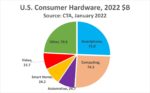
CES is Back – Partiallyby Bill Jewell on 01-13-2022 at 2:00 pmCategories: Events
CES (formerly the Consumer Electronics Show) returned to Las Vegas, Nevada last week. In 2021, CES was remote due to the COVID-19 pandemic. On April 28, 2021, the Consumer Technology Association (CTA), the sponsor of CES, announced CES 2022 would be held in Las Vegas. On the date of the announcement new COVID cases in the U.S. were… Read More
By now most SoC designers are pretty familiar and comfortable with the use of Network on Chip (NOC) IP for interconnecting functional blocks. Looking at the underlying change that NOCs represent, we see the use of IP to supplant the use of tools for implementing a critical part of the design. The idea that ‘smart’ things are better… Read More
One aspect of received wisdom on AI has been that all the innovation starts in the big machine learning/training engines in the cloud. Some of that innovation might eventually migrate in a reduced/ limited form to the edge. In part this reflected the newness of the field. Perhaps also in part it reflected need for prepackaged one-size-fits-many… Read More
Lauro Rizzatti recently interviewed Jean-Marie Brunet, vice president of product management and product engineering in the Scalable Verification Solution division at Siemens EDA, about why hardware-assisted verification is a must have for today’s semiconductor designs. A condensed version of their discussion is below.… Read More
Walking the exhibit floors at DAC in December I spotted the familiar face of Anupam Bakshi, Founder and CEO of Agnisys, so I stopped by the booth to get an update on his EDA company. My first question for him was about the origin of the company name, Agnisys, and I found at that Agni means Fire in Sanskrit, one of the five elements.
The … Read More
Ansys and Keysight wanted to see if they could answer the question, If we put virtual cellphones in different locations in a city, can we predict what kind of 5G signal we’re going to get in those locations? To find out, they created and tested a detailed virtual model of a city, including a variety of 5G antennae, receivers, and transmitters… Read More


TSMC CoWoS versus Intel EMIB Semiconductor Packaging