When TSMC’s annual Open Innovation Platform Exposition takes place, you know it will be time to hear about designs starting on the most advanced nodes. This year we were hearing about 7nm and 5nm. These newer nodes present even more challenges than previous nodes due to many factors. Regardless of what kind of design you are undertaking at these nodes, clocking IP is essential. This IP is analog and has even trickier design constraints at these smaller nodes. Andrew Cole at Silicon Creations gave a presentation at the Exposition that provide a lot of insight into what is required to produce this important foundation IP.
Silicon Creations has delivered clocking IP, such as PLLs, that have been used literally billions of times on production chips. Achieving success on this many instances requires tremendous verification resources. One of the interesting parts of Andrew’s presentation discussed the size of their server farm that are used for AFS simulation. They have two sites with more than 2000 cores. The combined RAM is 15TB. They need over 2000 AFS licenses to run their SPICE simulations. Being analog guys, they have even added their own liquid cooling on the processors so they can overclock them.
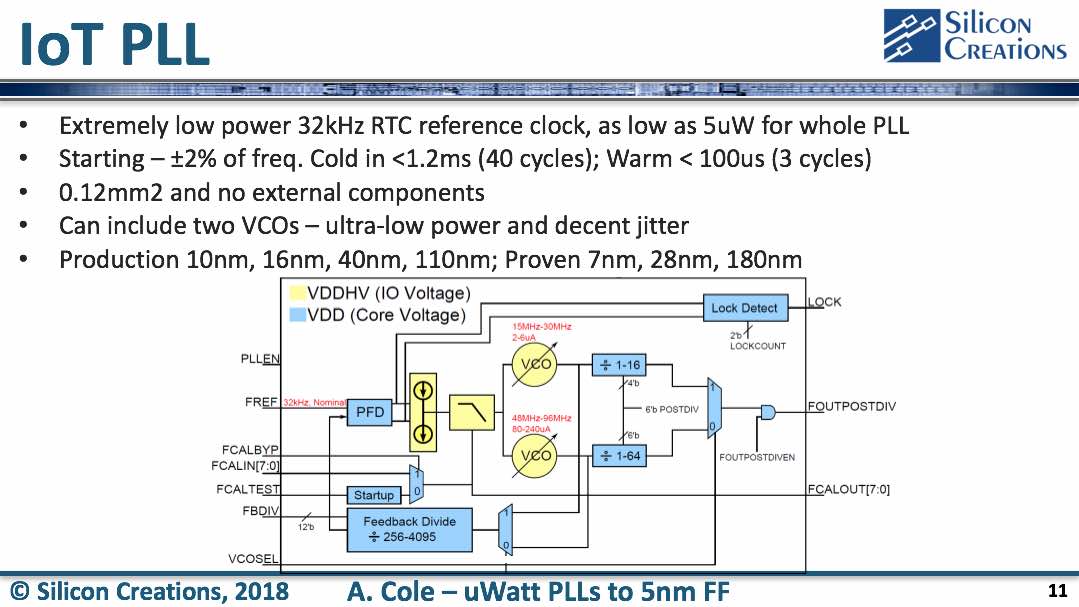
So why the need for such enormous resources? Andrew started by mentioning the application target for many of these ICs, which turns out to be IoT. He admitted that it is an over used term and has no good definition. However, it’s a useful shorthand for ICs that need to operate on low power, can start and stop quickly, have low leakage, and require few or no external components. Silicon Creations leverage TSMC’s low power processes: 180LP, 40ULP, 22ULL and FinFETs from 16nm to 5nm. These PLLs consume as little as 5uW and can start in as little as 3 clock cycles.

Andrew talked about how analog designs scale as processes shrink. They have seen their PLLs become about 8x smaller in the move from 180nm to 5nm. The limiting factor is noise which turns out to be proportional to kT/C. As such, capacitor values play a big role in determining noise. The other big challenge is wire resistance. With the significant relative increase in wire resistance, it is no longer possible to use lumped R for simulation. Silicon Creations has moved to performing simulation using fully distributed netlists for R and C. Add to this the need to use fully 3D aware tools, and the problem grows substantially. For an example PLL, it now takes 100 times longer to run post layout simulation for 5nm than it did at 40nm.
PLLs and SerDes face even more simulation obstacles. Their jitter requirements are on the order of 0.1ps. Clock cycles are ~100ps. System level activity can stretch out to 1ms, which is 10 orders of magnitude greater than the resolution needed to see jitter issues. Next, factor in the need to run Monte Carlo transient simulations to ensure good yield and it’s easy to see why Silicon Creations has had to scale up their server farm so extensively.
The next question is how well does all this simulation effort correlate to silicon. The answer is: quite well. For power, the mean and standard deviation match closely – sim: 3.02uA 1.5% to meas 3.15uA 1.6%. Below are the PLL fast locking plots.
![]()
Lastly, here is the graph for phase noise.
![]()
Few IP companies have as much experience and as many instances in the field as Silicon Creations. For digital design teams eager to take advantage of the benefits of 5nm, using proven and well designed and verified IP for clocking, Silicon Creations offers a compelling solution. Their 5nm solutions are taping out shortly. More information on the topic of advanced node analog clocking IP is available on the Silicon Creations website.
Share this post via:


Comments
There are no comments yet.
You must register or log in to view/post comments.