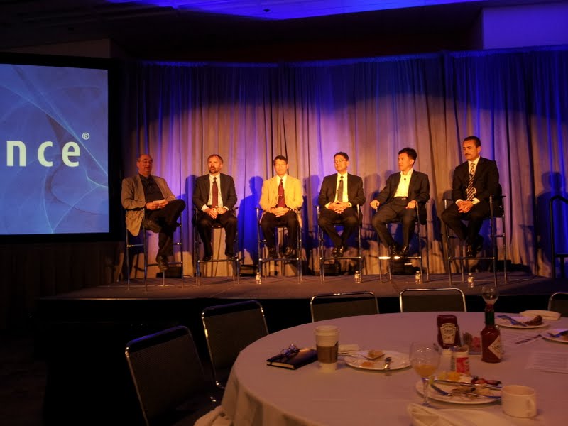
Wednesday morning I attended a panel discussion with: ARM, IBM, Cadence, GLOBALFOUNDRIES and Samsung.
The panelists all sang the same song of collaboration between EDA, IP and Foundry to enable 28nm, 20nm and even 14nm.
Steve Leibson, Cadence (host)
Gary Patton, IBM
technology scaling is not over, a few more decades are left with scaling although it becomes harder to do. It requires high R&D costs to bring to market. Collaboration at many levels is needed: materials, suppliers, equipment, virtual IDM with EDA and designers.
Disruptive innovations – Bipolar in the 1980s (hit power limit), planar CMOS in 1990s (gate oxide limit), Strain engineering in 2000s (HKMG), 2010 at the planar device limit (3D era of Devices like FinFET and packaging, need closer collaboration between EDA and design), 2020s at the Atomic dimension limit (nanowire devices, carbon nanotubes, 3d multi-chip stacking, photonics on chip).
Chi-Ping Hsu, Cadence
Lot of pressure on IC design tools to create a yielding chip. Statistical effects, well proximity effects, stress effects as process nodes continue from 180nm to 22nm. Nvidia quote on number of physical design team members at 28nm was 30X more than before.
“20nm design takes 5X the number of people compared to 65nm design. At 20nm we need 4-5 layout people for each 1 designer.”
More automation required on the full custom IC layout side to handle 20nm design.
EDA investment for new 20nm tool development is about $800M to $1.2B for the entire industry.
Dr. Dipesh Patel, ARM
Complexity of 28nm and 20nm rules is high, so give me rules that tell me what to do. Use these 20 or 30 layout patterns based on what will yield and have minimal variation effects. Look at the block level for density, not the cell level.
Voltage hasn’t been scaling so power remains high. Write assist in memory can raise the internal voltages to speed up cycle times.
Layout challenges: DPT coloring is new, how do we apply automation to do coloring?
SIgn-off complexity – 30 to 40 corners take a long time to simulate and analyze, automation required.
Metal stack is more complex at 20nm from design and extraction viewpoints.
Use multiple cycles of silicon validation at each node on Cores, cells, blocks, memory.
KM Choi, Samsung
Current mobile needs: smaller power and area, higher performance.
Process technology at 20nm and beyond requires use of TSV for wide IO paths. DPT needs to be decomposed automatically, router-aware. FinFET requires new SPICE model and cell structures.
20nm and 14nm test vehicles in fab now. Collaborate with IBM and Cadence.
Mojy Chian, GLOBALFOUNDRIES
Fabless foundry business is thriving and will continue to grow in size and profits, however the engagement model will be changing. Foundry business will have a 2X growth over the semiconductor business. 2011-2015 CAGR for semi is 5%, foundry is 10% and systems leading edge is 19%.
Driver for semi is mobility.
At 20nm the level of interdependence between foundry and IC design is extremely high. Virtual integration of IDM model: Foundry, Design, EDA.
Q&A:
Q: Is the foundry model broken at 20nm?
A: Mojy – no, the economics is still there, foundry and design are distinct. We just need to rely, and plan closer.
Choi – both IDM and Foundry. The foundry model isn’t broken, we need closer relationships.
Hsu – we’ve done horizontal segmentation as an EDA industry, where the R&D is amortized across many users. Vertical re-integration is required to be successful.
Collaboration must be started years ahead of production date from now on. 2.5 to 3 years before tape out we need collaboration between foundry and design.
Cadence tools completed 25 test chips for 20nm so far.
Q: Gabe – Can the fabs make money at 20nm and 14nm nodes?
A: Mojy – Two factors: we see consolidation in industry with high volume products, mobility is driving and China/India geographies are yet to be developed. Future looks bright.
Patel – new nodes always cost more at first, then provide better economics eventually as learning occurs.
Choi – history shows that semi costs come down.
Q: What does 14nm require?
A: Patton – presume that 14nm may use EUV but not demand it. Prescriptive design rules needed. More DPT needed. Dipole self assembly techniques in research now.
Choi – more than one 14nm development underway. EUV would be useful, but not required.
Chian – collaborating with IBM on EUV, interest is high. Industry is driven by performance per dollar, so when will EUV become economically viable?
Q: What effect does FinFET have on SoC designs?
A: Patel – IP will be created so that the user has a cell library and memory compiler, so don’t worry about the details. Yes, the IP will be more complex especially for analog and fixed device widths.
Hsu – full custom designers will have to learn about FinFET requirements.
Q: At 14nm how will collaboration work?
A: Chian – we compete for the same business and customers, however we collaborate on process development issues. GLOBALFOUNDRIES will have only one version of 28nm library, not multiple.
Patton – multi sourcing is good for business.


Comments
5 Replies to “Collaboration at 28nm, 20nm and 14nm”
You must register or log in to view/post comments.