Array
(
    [content] => 
    [params] => Array
        (
            [0] => /forum/index.php?threads/primary-contributors-to-wafer-fab-cycle-time-which-process-steps.18246/
        )

    [addOns] => Array
        (
            [DL6/MLTP] => 13
            [Hampel/TimeZoneDebug] => 1000070
            [SV/ChangePostDate] => 2010200
            [SemiWiki/Newsletter] => 1000010
            [SemiWiki/WPMenu] => 1000010
            [SemiWiki/XPressExtend] => 1000010
            [ThemeHouse/XLink] => 1000970
            [ThemeHouse/XPress] => 1010570
            [XF] => 2021370
            [XFI] => 1050270
        )

    [wordpress] => /var/www/html
)

Primary contributors to wafer fab cycle time (which process steps?)

jms_embedded

Active member
I am trying to find some order-of-magnitude estimates for the various steps in wafer fabs, and am wondering which are the biggest contributors to cycle time.

I've found various numbers for days per mask layer in published literature but they're generally in the 1-2 DPML range, and with X-factors in the 3-5 range that puts the raw processing time per layer somewhere in the 5-16 hour range, with queueing time making up the rest.

I've found various product brief / press releases from equipment manufacturers like ASML, Nikon, AMAT, Lam Research, etc. for DUV/EUV scanners, chemical vapor deposition tools, etchers, inspection machines, etc. and they're all in the 50 - 300 WPH range for throughput, but no numbers on latency. (example: even if the fastest scanners are 300WPH = 12 seconds per wafer, maybe the wafer has to wait for the entire lot before it can move on to the next process step, which means 12 s * 25 = 5 minutes per lot... but even if there are 5 lots waiting in a queue behind it, that's only 25 minutes which is small compared to the total raw processing time.)

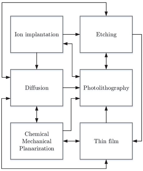
What about ion implantation / diffusion furnaces? Do these take longer? (I'm assuming diffusion furnaces might take several hours just due to the slow nature of heating/cooling and the need to avoid rapid thermal shock.) If so, do they contribute the most to raw process time and/or queueing time?

If anyone has some references they could point me at, I would appreciate it. (I suspect none of the IDMs/foundries publish their numbers, but someone must have a rough order of magnitude in a book or article somewhere)

The only tangible hints I found were in a 1998 article by Donald Martin from IBM (https://ieeexplore.ieee.org/document/731385) which mention "a six-hour furnace operation" and "20-minute ion implant" as hypothetical examples (and later another hypothetical furnace step with "a raw process time of four hours") and this section on major contribution to X-factor, where "WETS" perhaps = wet bench.

1687721376573.png
 
https://semiengineering.com/battling-fab-cycle-times/ -- not much for individual steps, but a great overview

You might find these papers interesting, showing the very long cycle times in practice, while the raw processing time for logic chips may indeed sum to 24 hours. You may need to add batch preparation times on the machines, though ideally the tools could do that while the chips they are preparing for are in a prior step. In practice it seems such just-in-time is not always happening.


an oldie, with some interesting numbers per wafer layer including process itemization https://www-physics.lbl.gov/~spieler/physics_198_notes/PDF/VIII-2-c-fab.pdf
a real oldie with data - Measurement and Improvement of MAnufacturing Capacities (MIMAC) (Fowler and Robinson 1995)

I have seen somewhere that about 2/3rds of all time is spent in transport or transport buffers, and I suspect that does not include queue time for foups docked at machines.
Given the large number of papers completely missing data on machines I suspect the real numbers are NDA by the manufacturers as well as by the Fabs.
 
https://semiengineering.com/battling-fab-cycle-times/ -- not much for individual steps, but a great overview
I've read that one before, but on a fresh read I picked up on something new: (my emphasis)
All of this adds up. “If you are doing triple patterning on some layers, and you have 50 to 60 layers, this takes a lot of time. You have all the waiting time for each of those steps. The real battle on cycle time is trying to reduce that waiting time,” UC Berkeley’s Leachman said. “One wafer doesn’t leave until all of the wafers in the lot have gone through the whole pipeline. Even though it’s one minute per wafer under the scanner, it still could be 45 minutes from when they start that lot and the robot can take the lot away.”

You might find these papers interesting, showing the very long cycle times in practice, while the raw processing time for logic chips may indeed sum to 24 hours.

...

I have seen somewhere that about 2/3rds of all time is spent in transport or transport buffers, and I suspect that does not include queue time for foups docked at machines.

Hmm, seems like raw processing time should be shorter than that. The X-factor numbers I've read in various papers are all around the 2.5 - 5 range (meaning total cycle time is 2.5 - 5.5x raw processing time) so RPT seems like it should be roughly in the 6-18 hr range (if DPML = 1-2 days at high loading). I'm just not sure how RPT and queueing time break down.

an oldie, with some interesting numbers per wafer layer including process itemization https://www-physics.lbl.gov/~spieler/physics_198_notes/PDF/VIII-2-c-fab.pdf
Huh, neat. Reminds me of Terry Holdt's notes on the MOS Technology "019" process used for the 6502: https://www.team6502.org/the-holdt-archives.html particularly the notes and run sheet. (Of course, I'm not a process engineer so I don't really pick up on the details.)

I'll look through the papers you cited -- thanks!
 
300mm wafers move from tool to tool in standardised FOUPs (Front Opening Unified Pod) usually of 25 wafers (may be 13).
Production is really a batch process even if some tools are single wafer processing. So indeed you have time spent to serialise the process and then parallelise the transport.
And a lot of issues are coming from interacting production lots with different recipes that make just simple queuing complex. Not mentioning unexpected tool issues.
 
Good catch on that point about raw time on a device per wafer vs. the raw time of the whole foup batch. And I have heard that multi exposure can batch more than 1 foup in order to minimize the wear caused by frequent mask and illumination changes in the machine. They may want to change the mask only once per 100 wafers instead of once per 25, so the total latency at that tool is magnified both by number of exposures and by the larger batch.
 
And a lot of issues are coming from interacting production lots with different recipes that make just simple queuing complex. Not mentioning unexpected tool issues.
I saw that in some of the published papers. Is this done in a just-in-time fashion where a tool may purge and load a new recipe while the batch is finishing up elsewhere, or do they run very conservative and wait until the wafers are queued before they adjust?

It occurs to me that as there is all this talk of excess capacity at least some of the fabs should see an opportunity to run at lower latency. The industry has evolved to minimize capex (minimizing equipment) while accepting cycle times exceeding 100 days on recent processes, but I've seen data that at least 30 days are trimmed off the cycle for hot lots. But if fabs need to profit at 70 to 80% utilization it will make sense for them to compete on better delivery schedules. There sure seems great potential for that, likely much more than 30 days if the fab rethinks to optimize latency. Time is money to most customers.
 
Where does the WIP tend to dominate in a fab, on average? Is it well-distributed in front of all tools? Or dominated by pileup in front of litho? This seems likely if lithography is the dominant bottleneck, but hard for me to understand with a throughput of 300 wafers per hour (12 seconds)... if 18-36 hours per mask layer is queue time, and even 10% of WIP is in front of lithography, that's 1.8 - 3.6 hours = 540 - 1080 wafers in a queue in front of lithography, which seems like a high number.
 
A well run fab has no bottlenecks in front of litho, it is build to have uniform throughput and you do not buy one tool more or less than necessary to maximise overall use. Underinvesting and creating bottlnecks is very quickly anti-economic and you do not have more or less depo/etch/clean equipment that your litho can handle. But queues in front of equipment are inevitable, what you want is that they are managed so that average utilisation do not drop due to fluctuations. Just in time and zero queue is a sure way that at the first unforecasted event all goes belly up.
And looking at published tools throughput is a bit as looking at published car fuel consumptions: ballpark at best. Hot lots are the nigthmare of the fab manager because for one lot that shave 30 days you have tens of lots that adds a few days to their cycle and customers that scream. In order to have the hot lot to be pushed through, you may have tools on hold for hours to make sure they are ready for when the lot arrives and so your average utilisation rate decrease. It requires a lot of people signing off.....
 
I appreciate the 1st-person reporting, but some of those things are puzzling. If a tool goes down you lose the batch in progress. If the upstream wafers are queued, or in some other tool, then the question is pretty much the same - can an alternate tool be scheduled? Obviously delays will occur - it just is not obvious that queues in front of the tool fix anything.

That is separate to queues which match routine fluctuations. Yes, you need queues to mismatch between rates on tools in a chain.

However, the situation we have is > 95% queueing, < 5% wafers in a tool actually processed. Even for hot lots. This is an extreme seller's market scenario where they build, as you say, exactly the number of machines they need to keep them all at capacity, and no more. Or maybe an Apple scenario where one customer floods the fab for a few months. A balance of 95% in favor of fab profits at the expense of customer screams in most industries would be seen as alarming, not status quo.

I suspect one consequence of pouring money into new fabs for supply chain diversity will also be to incentivize fabs (and tool makers) to figure out how to eliminate the amazing queues. If you need to make customers happy, it makes sense to stop them needing to scream.
 
What are the longest steps in the fabrication process? furnace anneals?

...and why would wet bench have a long queue / high variability?
 
Last edited:
That is separate to queues which match routine fluctuations. Yes, you need queues to mismatch between rates on tools in a chain.
Problem is that a semiconductor fab is not one long chain of machines after each but that the same tools are used for different steps in the processing of a lot. And these are not only wafer processing tools but alos metrology like CD-SEM, ellipsometry, etc. Problem is that the cycles in between such steps are different depending on where you are in the processing of the wafer. Also sometimes during metrology things are seen out of spec and individual steps are reworked. At imec the inspection/metrology was seen not as a separate lot turn but included in the lot turn of a process step although they happen on two different tiools.
You need buffers in between tools to maximize utilisation rate of the individual tool. At some point reducing the buffers will reduce utilization rate of the tools due to varying arrivel times after previous use of the tool on the batch. Depreciation and maintenance cost are major cost driver so reduced utilization rates means less profit.
 
Back
Top