Array
(
    [content] => 
    [params] => Array
        (
            [0] => /forum/index.php?threads/huawei-patent-shows-6x-multi-patterning-surpassing-euv-resolution-without-euv.19903/page-3
        )

    [addOns] => Array
        (
            [DL6/MLTP] => 13
            [Hampel/TimeZoneDebug] => 1000070
            [SV/ChangePostDate] => 2010200
            [SemiWiki/Newsletter] => 1000010
            [SemiWiki/WPMenu] => 1000010
            [SemiWiki/XPressExtend] => 1000010
            [ThemeHouse/XLink] => 1000970
            [ThemeHouse/XPress] => 1010570
            [XF] => 2021370
            [XFI] => 1050270
        )

    [wordpress] => /var/www/html
)

Huawei Patent Shows 6x Multi-Patterning Surpassing EUV Resolution Without EUV

It's not that simple. Samsung exists too. So while the West diverts logic to Samsung and Intel, China would have no memory and storage suppliers to buy from. CXMT and YMTC can't meet all their needs, especially with broadened trade restrictions a Taiwan blockade would cause.
A huge chunk of Samsung and SK Hynix memory production is in China. Especially SK Hynix. Look it up.
In case of conflict the Chinese would just hand over the South Korean factories to Chinese companies so they would operate them. And they would add to their production.
 
Samsung has NAND production there, but no DRAM. SK Hynix has 40% DRAM there, and NAND. It still would be short China's needs. Not sure a fab would work very well without any supplier support, and Korea support.
 
They would work as well as China's existing fabs which also use Western equipment from pretty much the same suppliers. It would require reorganizing production to fit the new products the fabs would produce but the buildings, people, and tools would be there.

Some of Micron's largest memory fabs are also at Taiwan. The ones they bought from Inotera and Rexchip. They would be gone in case of conflict.

Most of Micron's fabs are in Asia. Taiwan, Singapore, and Japan. They do not have all their production in the US.

CXMT and YMTC also doubled their floorspace last year. Their expansions should be in production this year.
 
Last edited:
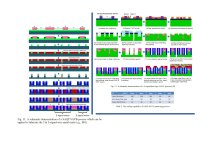
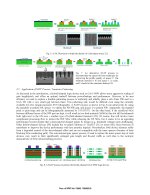
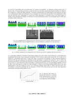
SPIE just published the papers from Advanced Lithography + Patterning. Here are a couple of pages, figures and table grasped from the 7x paper (see below) by Westlake University. Obviously, our industry should seriously think about if we really need high-NA EUVL. TSMC may again make a right decision (vs. Intel).

Paper: Mandrel/Spacer Engineering Based Patterning and Metallization Incorporating Metal Layer Division and Rigorously Self-Aligned Vias & Cuts (SAVC)
 

Attachments

  • SAQP_SASP.jpg
    SAQP_SASP.jpg
    471.6 KB · Views: 76
  • Page6.jpg
    Page6.jpg
    608.2 KB · Views: 53
  • Page10.jpg
    Page10.jpg
    637 KB · Views: 54
Last edited:
SPIE just published the papers from Advanced Lithography + Patterning. Here are a couple of figures and table grasped from the 7x paper by Westlake University. Obviously, our industry should seriously think about if we really need high-NA EUVL. TSMC may again make a right decision (vs. Intel).
If our industry could make chips with powerpoint the answer would be obvious, not EUV. Given the order book for high NA EUV, the real answer was made years ago to go down that road.
 
Of course it's not only ppt, they reported some preliminary experiment results to show its feasibility. High-NA EUV is not the only path. Several different approaches to scale down exist, including SADP EUV (low NA) patterning proposed by Imec. Intel booked some high-NA tools. I heard TSMC did not and Samsung might or might not. You are welcome to correct me if my information is incorrect.
 
If our industry could make chips with powerpoint the answer would be obvious, not EUV. Given the order book for high NA EUV, the real answer was made years ago to go down that road.
High-NA EUV could very well be a bad decision. There is no High-NA EUV print data. But we have enough information from existing EUV to show even that was questionable.
 
As for any other process, is not a matter of "best technology" but of "what does it well enough at the right cost". Then the issues are "well enough" and "right cost" that may differ among players. EUV certainly does it well enough (even "better" arguably) and cheaper than multi-patterning at 7, 5 and 3nm for most of the current players. And when I say right cost, that includes the overall good die/wafer yield factored in, not just the pattern/etch process. I still remember a paper I (very marginally) contributed years ago showing excellent results of x-y pattern decomposition to use dual exposure in 193nm dry tools that was simply worthless with the introduction of 193i. ;)
Will EUV be the solution of choice for the next nodes is a debate to which Fred brings always good points but, I think, it is still from over and depending on multiple issues from materials, blanks, reticle patterning to computational tools and litho tools. But for the past ones the history is written and whoever will use other techniques will be economically at a disadvantage.
You assumed EUV got you out of multipatterning, but that is not the case, even for High-NA (i.e., stitching of multiple exposures).
 
You assumed EUV got you out of multipatterning, but that is not the case, even for High-NA (i.e., stitching of multiple exposures).

Agreed, but definitely the number and cost of overall processing steps went down with EUV introduction at 7 and 5nm. Will that still be true is part of the question I think. Not so much into litho as at one time, but I think that the debate, for those that can have access to EUV, will be multipatterning with EUV vs multipatterning with High-NA not re-introduction of 193i. Immersion will be for those that cannot have EUV. But it is an opinion, just a thumb in the air, not a serious analysis as yours. One element I am at a loss to evaluate is the impact of computational solutions to adapt the pattern to the optics. Oversimplyfing for the sake of argument: any litho equipment is a low pass transfer function so, provided I can inverse it, I should be able to have the needed input to get the desired output. Given what whe know of the tool and the compuational capability, can I calculate the inverse ? Can I then make a mask for it ? Once was impossible, it is still so today? What in future ?
 
Agreed, but definitely the number and cost of overall processing steps went down with EUV introduction at 7 and 5nm. Will that still be true is part of the question I think.
I am not sure that is significantly the case, since EUV didn't get on all layers, especially 7nm. DUV double patterning still cheaper than EUV. On 5nm, the cost overall still went up since there was EUV and DUV multipatterning. I think there is still a common misconception that resolution is strictly determined by wavelength and NA. Actually for EUV, it's electrons and stochastics. Those can't be inverted, at least currently.
 
Agreed, but definitely the number and cost of overall processing steps went down with EUV introduction at 7 and 5nm. Will that still be true is part of the question I think. Not so much into litho as at one time, but I think that the debate, for those that can have access to EUV, will be multipatterning with EUV vs multipatterning with High-NA not re-introduction of 193i. Immersion will be for those that cannot have EUV. But it is an opinion, just a thumb in the air, not a serious analysis as yours. One element I am at a loss to evaluate is the impact of computational solutions to adapt the pattern to the optics. Oversimplyfing for the sake of argument: any litho equipment is a low pass transfer function so, provided I can inverse it, I should be able to have the needed input to get the desired output. Given what whe know of the tool and the compuational capability, can I calculate the inverse ? Can I then make a mask for it ? Once was impossible, it is still so today? What in future ?
I guess you can mathematically do something like inverse transform to calculate what the exact wavefront at the mask surface should be to match your target pattern, but the problem is that both phase and intensity of thus calculated "mask" wavefront are continuous or analog signals (spatial functions). Today's analog/reflective SLM micromirror array probably allows you to control 32-64 levels of phase/position to mimic the continuous phase map, but I am not aware of any technique that can simultaneously control/mimic the continuous light intensity distribution at the mask surface. All we can do today is to approach them as close as possible to minimize the errors. The other problem is the defined "mask" region according to the inverse transform will be (-infinity, +infinity), but the mask size is limited and some spectrum will still be lost. If both phase and intensity signals of a large enough mask can be accurately controlled, that means one can construct any pattern they want through the inverse transform. Then the diffraction limit will disappear and this will definitely lead to a Nobel prize.
 
Last edited:
DUV double patterning still cheaper than EUV
Doubt that it is always the case, otherwise EUV would not sell. For some layers it is clearly an economic advantage somehow.

Actually for EUV, it's electrons and stochastics. Those can't be inverted, at least currently.
Excellent point. That was the oversimplification that fails the moment we deals with stochasticity. At that point we move from classical to quantum optics and the inversion does not make sense anymore.

The other problem is the defined "mask" region according to the inverse transform will be (-infinity, +infinity), but the mask size is limited and some spectrum will still be lost. If both phase and intensity signals of a large enough mask can be accurately controlled, that means one can construct any pattern they want through the inverse transform.
That was the reason I pointed out the feasibility of the mask. Clearly in reality we will always have finite domains being in the frequency, phase or spatial one so all solutions will be approximate. If I re-express my point, the question is if that approximation will be enough to use one of the current tools/techniques to image the requirements of 1nm and how much below. Or do we need to look for other tools (EUV High-NA, e-beams, ..) because the barrier is not avoidable.
The point I still have problems with it is the fact that you can be economically competitive and keep being so just going the multipattern 193i way, not its technical doability.
 
Doubt that it is always the case, otherwise EUV would not sell. For some layers it is clearly an economic advantage somehow.
EUV had to be bought and subsequently used before the data was in, apparently. About the costs, some references below. Keep in mind, EUV resists are many times more expensive than DUV resists.

DUV vs EUV multipatterning (ASML 2019).png
Micron EUV vs Quadruple Patterning.png
 
Last edited:
Doubt that it is always the case, otherwise EUV would not sell. For some layers it is clearly an economic advantage somehow.


Excellent point. That was the oversimplification that fails the moment we deals with stochasticity. At that point we move from classical to quantum optics and the inversion does not make sense anymore.


That was the reason I pointed out the feasibility of the mask. Clearly in reality we will always have finite domains being in the frequency, phase or spatial one so all solutions will be approximate. If I re-express my point, the question is if that approximation will be enough to use one of the current tools/techniques to image the requirements of 1nm and how much below. Or do we need to look for other tools (EUV High-NA, e-beams, ..) because the barrier is not avoidable.
The point I still have problems with it is the fact that you can be economically competitive and keep being so just going the multipattern 193i way, not its technical doability.
Fred is pessimistic to EUV from day one. He raised questions about stochastic, through slit best focus drift, mask 3D effect, blurring effect in EUV generated 2nd electrons....., even though there are millions EUV wafers printed. There are difference between engineering works and scientific studies. He is right, but it seems work arounds have been validated and implemented in the field.
 
In the EUV-vs-DUV cost debate, we should also consider that EUV saves on cycle time. In the R&D phase, especially, it is important to get quick learning and to avoid long cycle times. One EUV layer may not make a big difference, but if a flow contains too many multiple exposures, the latter will add up and significantly slow down development. As long as there is some level of competition between foundries, faster development time will pay off. This must enter the cost equation when comparing litho solutions.
 
Unfortunately everybody is dragged into this semiconductor subsidy race now,with government all over the global giving out more and more subsidy as we speak.

You need only one weakest link in the very long, and very complex chain of subsidised companies supplying the factory to fail for the whole subsidised supply chain to stall.

This is why subsidy of complex industries is an all or nothing affair. I remember how Japanese semiconductor grade silicon producers managed to stop the entirety of Japanese semi industry once they lost subsidies.
 
Back
Top