Array
(
    [content] => 
    [params] => Array
        (
            [0] => /forum/index.php?threads/huawei-tests-brute-force-method-for-making-more-advanced-chips.19883/
        )

    [addOns] => Array
        (
            [DL6/MLTP] => 13
            [Hampel/TimeZoneDebug] => 1000070
            [SV/ChangePostDate] => 2010200
            [SemiWiki/Newsletter] => 1000010
            [SemiWiki/WPMenu] => 1000010
            [SemiWiki/XPressExtend] => 1000010
            [ThemeHouse/XLink] => 1000970
            [ThemeHouse/XPress] => 1010570
            [XF] => 2021370
            [XFI] => 1050270
        )

    [wordpress] => /var/www/html
)

Huawei Tests Brute-Force Method for Making More Advanced Chips

Daniel Nenni

Admin
Staff member
fd68948f21fca13a28783f66bfecea59

Huawei Tests Brute-Force Method for Making More Advanced Chips

(Bloomberg) -- Huawei Technologies Co. and a secretive chipmaking partner in China have filed patents for a low-tech but potentially effective way to make advanced semiconductors, raising the prospect that China could improve chip production techniques despite US efforts to halt its progress.

The companies are developing technologies that involve self-aligned quadruple patterning, or SAQP, and should reduce their reliance on high-end lithography, according to patent filings to the Chinese intellectual property authority. That may allow them to produce advanced chips without ASML Holding NV’s state-of-the-art extreme ultraviolet lithography equipment. Netherlands-based ASML, the sole provider of EUV machines, cannot sell them into China because of export controls.

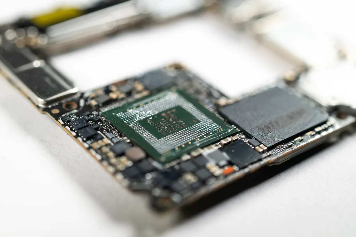
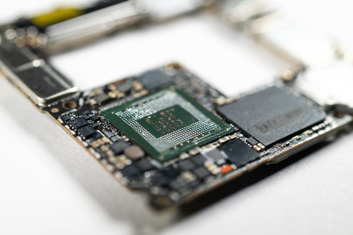
Quadruple patterning is a technique for etching lines on silicon wafers multiple times to increase transistor density — and therefore performance. Huawei’s patent application, released on Friday, describes a method that uses the technology to make more sophisticated semiconductors. “Adoption of this patent will increase the design freedom of circuit patterns,” said the filing to China National Intellectual Property Administration.

SiCarrier, a state-backed chipmaking gear developer that works with Huawei, was granted a patent that involves SAQP, in late 2023. Its patent employs deep ultraviolet lithography, or DUV, chipmaking machines and the SAQP technology to achieve certain technical thresholds seen on 5 nanometer chips, according to its filing. The practice can avoid the use of EUV machines while reducing manufacturing cost, it said.

Quadruple-patterning technology is good enough for China to make chips at 5nm, but China still needs to get its hands on EUV machines in the long run, according to Dan Hutcheson, vice-chairman at research firm TechInsights. “It can mitigate them, but not completely overcome the technical issues of not having EUV,” he said.

Leading chipmakers like Taiwan Semiconductor Manufacturing Corp. use EUV machines to produce advanced chips because they have the highest production yields — meaning the cost per chip is minimized. If Huawei and its partners use alternative methods for semiconductor production, their cost per chip may be higher than the industry’s standards.

The most advanced chips now in commercial production use 3nm technology, including chips that TSMC makes for the likes of Apple Inc. China is currently capable of making 7nm chips, two generations behind, but advancing to 5nm would put it only a single generation behind the global leaders.

The US and its allies have been tightening China’s access to semiconductors and chipmaking equipment for years, with the Biden administration arguing such controls are necessary for national security. That includes bans on the export of ASML’s EUV chipmaking machines and Nvidia Corp.’s most powerful graphic processors, used for training artificial intelligence services.

But Chinese companies are investing billions to develop their domestic chip capabilities and Huawei unveiled a breakthrough smartphone last year that was powered by an advanced 7nm processor. That suggested the country’s tech sector is making progress despite the efforts of the US, the Netherlands and Japan.

In response, the Biden administration is looking for additional means to contain China’s progress. It’s pressing allies like South Korea and Germany to join the effort, and is considering blacklisting even more Chinese chip firms linked to Huawei, including SiCarrier.

A cohort of Chinese chip equipment makers including Naura Technology Group Co. and Advanced Micro-Fabrication Equipment Inc., are also looking into complementing multiple patterning technology with etching systems to produce 7nm or more advanced chips because EUVs are out of reach, according to a memo authored by Citigroup’s analysts including Jamie Wang and Kevin Chen.

“Chinese semiconductor companies mainly resort to SAQP to produce advanced chips, which could increase the density of etching machines in China,” it said.
Beijing this year has thrown its backing fully behind the nation’s most prominent suppliers of chipmaking gear. This month, Premier Li Qiang visited the offices of Naura Technology in a widely publicized personal tour, usually orchestrated to signal central government support.

 
23nm M0 near the limit of SAPQ lines, SAPQ vias to get to the contacts and from M1->M0, SAPQ for block masks that need to be assembled in reverse, self aligned contacts and everything that entails when gate pitch gets into the 40s like with N3. I will be an old man before that process yields, and dead in my grave before a chip designer can even comprehend the design rules enough to port an arm core (not literally just for dramatic effect). If/when a process like this comes out (since I suspect technical limitations will push for a more relaxed BEOL or DSA to make it less miserable), SMIC really does deserve some kind of standing ovation. No matter how long it takes, it would be an amazing achievement even if non litho companies illegally send their best gear to China. Also as someone who really likes self aligned features, it would warm my heart to see one node with so many ;)

As a side note I wonder why is it Huawei and not SMIC doing this research? Also I wonder why they don’t try to develop a SALE^4 process? Alot of exTSMC folks work at SMIC so they should be very familiar with SALELE.
 
The said patent CN117080054 is actually not SAQP per se but SADP-LE (cut)-SADP-LE(cut), which might just be an option for them. However, the patent explicitly referred to a target of 28 nm pitch (basically N5 reference). Can they get away with LE cut instead of LELE cut as I would have expected by default?

The SiCarrier entity is not Huawei or SMIC but perhaps tapped to be a contributor. https://www.sicarrier.com/
 
First single-material SAQP paper was published by AMAT in 2011 SPIE Adavanced Lithography, but they didn't apply for a patent. So it has been used in FEOL fin step without any issue. The dual-material SAQP patent to use etching selectivity to solve the EPE issue, however, to my knowledge was invented in 2015 and patented by Peking University in 2017 (US patent: 9679771 B1). I guess Intel used it to at least fabricate N10 M1 (see TechInsight report), but Intel did not pay for it, for which PKU was discussing a law solution! There are two SAQP patents that are hot this week. The SiCarrier SAQP variant is quite normal and will not be dicussed here; the other one is from HiSilicon (CN 117751427 A: 自对准四重图案化半导体装置的制作方法以及半导体装置), which extended 2x SALELE to 4x SALELELE..., the problem is that it requires too many masks (7-8), and the yield may be close to 0! The critical issue is not density multiplicaion such as 2x or 4x, it is the very small cuts/blocks and vias (12-16nm) that need to be self-aligned, otherwise they will miscut/mis-connect the wrong metal lines. The real shock is HiSilicon has a 7x (SASP which can drive down metal pitch to 12nm) patent that incorporate self-aligned vias & cuts (WIPO patent application # CN2022/097621). Details of this patent was just disclosed in the paper titled "Mandrel/spacer engineering based patterning and metallization incorporating metal layer division and rigorously self-aligned vias & cuts (SAVC)” in 2024 SPIE Advanced Lithography + Patterning, and their amazing effort will be soon seen in Proc. of SPIE in May.
 
The real shock is HiSilicon has a 7x (SASP which can drive down metal pitch to 12nm) patent that incorporate self-aligned vias & cuts (WIPO patent application # CN2022/097621). Details of this patent was just disclosed in the paper titled "Mandrel/spacer engineering based patterning and metallization incorporating metal layer division and rigorously self-aligned vias & cuts (SAVC)” in 2024 SPIE Advanced Lithography + Patterning, and their amazing effort will be soon seen in Proc. of SPIE in May.
 
First single-material SAQP paper was published by AMAT in 2011 SPIE Adavanced Lithography, but they didn't apply for a patent. So it has been used in FEOL fin step without any issue. The dual-material SAQP patent to use etching selectivity to solve the EPE issue, however, to my knowledge was invented in 2015 and patented by Peking University in 2017 (US patent: 9679771 B1). I guess Intel used it to at least fabricate N10 M1 (see TechInsight report), but Intel did not pay for it, for which PKU was discussing a law solution!
Around the time of this patent https://patents.google.com/patent/US9679771B1/en?oq=9679771 TEL and imec were publishing about the same or similar technique at SPIE 2017. Has this been licensed to TEL or others?
 
I am not clear about the TEL or Imec patents, apparently they had done a lot of follow-up work since 2017. Here are some references about single-material SAQP/SATP ([1-3]) for density multiplication and dual-material SAQP/SAMP for solving EPE issue [4-6]:

[1] P. Xu, Y. M. Chen et al., “Sidewall spacer quadruple patterning for 15-nm half-pitch,” Proc. of SPIE, Vol. 7973, 79731Q, 2011.
[2] Y. Chen, P. Xu et al., “Self-aligned triple patterning for continuous IC scaling to half-pitch 15nm,” Proc. of SPIE, Vol. 7973, 79731P, 2011.
[3] Y. Chen, Y. M. Chen et al., “Spatial frequency multiplication techniques towards half-pitch 10 nm patterning,” Proc. of SPIE, Vol. 7973,79731T, 2011.
[4] T. Han, H. Liu, Y. Chen, “A solution to reduce the effect of edge-placement errors by selective etching and alternating-material self-aligned multiple patterning, Part I: edge-placement yield modeling and optimization,” International Conference on Micro- and Nano-Engineering (MNE), The Hague, Netherlands, September, 2015.
[5] T. Han, H. Liu, Y. Chen, “A paradigm shift in patterning foundation from frequency multiplication to edge placement accuracy - a novel processing solution by selective etching and alternating-material self-aligned multiple patterning,” Proc. of SPIE, Vol. 9777, 977718, 2016.
[6] T. Han, H. Liu, Y. Chen, “Process development and edge-placement yield modeling of alternating-material self-aligned multiple patterning,” Journal of Micro/Nanolithography, MEMS and MOEMS, 15(3), 031609, 2016.
 
The dual-material SAQP patent to use etching selectivity to solve the EPE issue, however, to my knowledge was invented in 2015 and patented by Peking University in 2017 (US patent: 9679771 B1). I guess Intel used it to at least fabricate N10 M1 (see TechInsight report), but Intel did not pay for it, for which PKU was discussing a law solution!
I guess they felt the damascene-based process was different.
 
I am not clear about the TEL or Imec patents, apparently they had done a lot of follow-up work since 2017. Here are some references about single-material SAQP/SATP ([1-3]) for density multiplication and dual-material SAQP/SAMP for solving EPE issue [4-6]:

[1] P. Xu, Y. M. Chen et al., “Sidewall spacer quadruple patterning for 15-nm half-pitch,” Proc. of SPIE, Vol. 7973, 79731Q, 2011.
[2] Y. Chen, P. Xu et al., “Self-aligned triple patterning for continuous IC scaling to half-pitch 15nm,” Proc. of SPIE, Vol. 7973, 79731P, 2011.
[3] Y. Chen, Y. M. Chen et al., “Spatial frequency multiplication techniques towards half-pitch 10 nm patterning,” Proc. of SPIE, Vol. 7973,79731T, 2011.
[4] T. Han, H. Liu, Y. Chen, “A solution to reduce the effect of edge-placement errors by selective etching and alternating-material self-aligned multiple patterning, Part I: edge-placement yield modeling and optimization,” International Conference on Micro- and Nano-Engineering (MNE), The Hague, Netherlands, September, 2015.
[5] T. Han, H. Liu, Y. Chen, “A paradigm shift in patterning foundation from frequency multiplication to edge placement accuracy - a novel processing solution by selective etching and alternating-material self-aligned multiple patterning,” Proc. of SPIE, Vol. 9777, 977718, 2016.
[6] T. Han, H. Liu, Y. Chen, “Process development and edge-placement yield modeling of alternating-material self-aligned multiple patterning,” Journal of Micro/Nanolithography, MEMS and MOEMS, 15(3), 031609, 2016.
I look forward to reading your SPIE 2024 papers!
 
It should be available soon in SPIE digital library. Keep it in mind the multi-color self-aligned block (renamed by TEL and Imec) is actually self-aligned cut (dielectric)+metal filling (damascene), and the key idea of self-aligned cut is using different materials arranged in an alternating order and applying selective etching/cut to solve the EPE issue, which was an innovation back in 2015 (now well known) and covered by PKU patent. I think neither TEL/Imec nor Intel should take this credit and claim it's their own developed technology.
 
Back
Top