Array
(
    [content] => 
    [params] => Array
        (
            [0] => /forum/index.php?threads/intel-to-get-8-5b-from-the-chips-act.19869/
        )

    [addOns] => Array
        (
            [DL6/MLTP] => 13
            [Hampel/TimeZoneDebug] => 1000070
            [SV/ChangePostDate] => 2010200
            [SemiWiki/Newsletter] => 1000010
            [SemiWiki/WPMenu] => 1000010
            [SemiWiki/XPressExtend] => 1000010
            [ThemeHouse/XLink] => 1000970
            [ThemeHouse/XPress] => 1010570
            [XF] => 2021370
            [XFI] => 1050270
        )

    [wordpress] => /var/www/html
)

Intel to get $8.5B from the CHIPS Act

blueone

Well-known member

“With this agreement, we are helping to incentivize over $100 billion in investments from Intel — marking one of the largest investments ever in U.S. semiconductor manufacturing, which will create over 30,000 good-paying jobs and ignite the next generation of innovation,” U.S. Secretary of Commerce Gina Raimondo notes in a release.
 

Biden-Harris Administration Announces Preliminary Terms with Intel to Support Investment in U.S. Semiconductor Technology Leadership and Create Tens of Thousands of Jobs

U.S. Department of Commerce Proposes up to $8.5 Billion in Potential Direct Funding for Intel Under President Biden’s Investing in America Agenda to Support Multiple Projects in Arizona, New Mexico, Ohio, and Oregon

Today, the Biden-Harris Administration announced that the U.S. Department of Commerce and Intel Corporation have reached a non-binding preliminary memorandum of terms (PMT) to provide up to $8.5 billion in direct funding under the CHIPS and Science Act to strengthen the U.S. supply chain and re-establish American leadership in semiconductor manufacturing. Leading-edge logic chips are essential to the world’s most advanced technologies like artificial intelligence, and this proposed funding would help ensure more of those chips are developed and made domestically. As President Biden highlighted in his State of the Union, the CHIPS and Science Act is charting a new course to manufacture critical technologies in America, lead the world in innovation, and create good jobs here in the United States. This is the Department of Commerce’s fourth PMT announcement under the CHIPS and Science Act.

Over the course of the next five years, Intel expects its investments in the United States to exceed $100 billion, as it expands capacity and capabilities in Arizona, New Mexico, Ohio, and Oregon, estimated to directly create over 10,000 manufacturing jobs and nearly 20,000 construction jobs. The Biden Administration’s proposed CHIPS investment, coupled with Intel’s investment, would mark one of the largest investments ever announced in U.S. semiconductor manufacturing. The PMT also includes approximately $50 million in dedicated funding to develop the company’s semiconductor and construction workforce. This builds upon Intel’s own workforce investments, totaling over $250 million in the past five years, as well as its strong partnerships with local communities, community colleges, universities, Historically Black Colleges and Universities (HBCUs), and apprenticeship programs.

“There is no one who cares more about revitalizing American manufacturing than President Biden, and today’s announcement is a massive step towards ensuring America’s leadership in manufacturing for the 21st century. With this agreement, we are helping to incentivize over $100 billion in investments from Intel – marking one of the largest investments ever in U.S. semiconductor manufacturing, which will create over 30,000 good-paying jobs and ignite the next generation of innovation,” said U.S. Secretary of Commerce Gina Raimondo. “This announcement is the culmination of years of work by President Biden and bipartisan efforts in Congress to ensure that the leading-edge chips we need to secure our economic and national security are made in the U.S.”

Leading-edge chips power the most sophisticated technology on the planet, including developing AI and building critical military capabilities. Intel’s process technologies such as Intel 18A and advanced packaging technologies, combined with its foundry services, would better enable U.S. companies to lead the AI industry by ensuring we have a domestic supply of these advanced chips.

“The CHIPS for America program will bring semiconductor manufacturing back to the U.S. and create a vital R&D ecosystem to keep it here,” said Under Secretary of Commerce for Standards and Technology and NIST Director Laurie E. Locascio. “The innovation sparked by this proposed investment would strengthen America’s technological and research leadership and significantly help enhance our nation’s manufacturing capacity while strengthening communities and creating good-paying jobs.”

“Today is a defining moment for the U.S. and Intel as we work to power the next great chapter of American semiconductor manufacturing innovation,” said Intel CEO Pat Gelsinger. “AI is supercharging the digital revolution and everything digital needs semiconductors. CHIPS Act support will help to ensure that Intel and the U.S. stay at the forefront of the AI era as we build a resilient and sustainable semiconductor supply chain to power our nation’s future.”

This proposed investment would deliver on the Administration's commitment to developing a robust domestic semiconductor ecosystem by reinforcing Intel's decades-long history in the United States. The investment will also enable the company to support industry-leading, U.S.-based fabless semiconductor companies with U.S.-based leading-edge production. The proposed CHIPS funding would strengthen all major technical processes for leading-edge chips to occur in the United States, including proposed investments in:
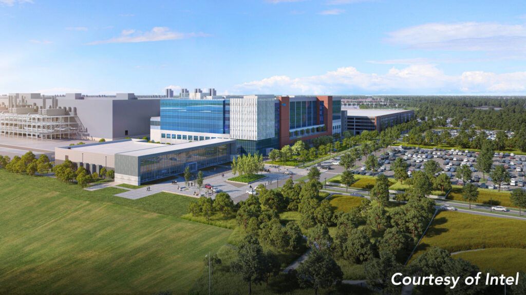
  • Chandler, Arizona: Construction of two new leading-edge logic fabs and modernization of one existing fab, significantly increasing leading-edge logic capacity, including high volume domestic production of Intel 18A – the company’s most advanced chip design that enables higher performing, leading-edge chips through RibbonFET gate-all-around transistors and PowerVia backside power delivery. The company will produce the first Intel 18A product, called Clearwater Forest, at its Arizona facilities. In 2022, Intel partnered with Maricopa County Community Colleges to launch a first-of-its-kind program with Intel employee-instructors to provide students an entry point into semiconductor technician careers. This investment will support 3,000 manufacturing jobs and 6,000 construction jobs.
  • Rio Rancho, New Mexico: Modernization of two fabs into advanced packaging facilities to close an important gap in the domestic semiconductor supply chain. When in full production, this facility will be the largest advanced packaging facility in the United States. To support engineering students in New Mexico, Intel established endowment scholarships at five colleges and universities and has supported STEAM education through investments, annual grants, and hands-on learning kits benefitting students living on indigenous lands. This investment will support 700 manufacturing jobs and 1,000 construction jobs.
  • New Albany, Ohio: Creation of a new regional chipmaking ecosystem, anchored by the construction of two leading-edge logic fabs, expanded leading-edge foundry capacity, and supply chain diversification. Intel has devoted significant resources to develop a pipeline of skilled workers in Ohio, funding over 80 institutions of higher education across the state, including community colleges, HBCUs, and universities. As part of this investment in Ohio, Intel’s design and build partner Bechtel signed a Project Labor Agreement (PLA) with the North America Building Trades Unions for the construction of the two facilities. This investment will support 3,000 manufacturing jobs and 7,000 construction jobs.
  • Hillsboro, Oregon: Investment in the premier hub of leading-edge development in the United States through the expansion and modernization of technology development facilities that will utilize the world’s first High NA EUV lithography equipment. The Gordon Moore Park campus at Ronler Acres in Hillsboro, Oregon is the heart of Intel’s innovation hub for leading-edge semiconductor research and technology development in the United States. These investments will further the company’s technological leadership and enable the continued development of new innovations. In 2022, Intel spent more than $4 billion with more than 500 suppliers across Oregon. This investment will support several thousand manufacturing and construction jobs.
Intel currently uses 100% renewable electricity in U.S. fabs and has achieved net-positive water status in its U.S. operations through efficient water management, water reuse, and, in collaboration with local communities, investment in water restoration in local watersheds. In addition, as part of its broader workforce investment program, Intel has committed to providing affordable, accessible, high-quality child care for its workers across its facilities. For U.S. employees, Intel will be increasing the reimbursement amount and duration for its back-up care program and adding additional access to discounted primary child care providers, as well as access to a vetted network of child care providers. In addition, Intel will pilot a primary child care reimbursement program for non-exempt employees.

In addition to the proposed direct funding of up to $8.5 billion, the CHIPS Program Office would make up to $11 billion in loans – which is part of the $75 billion in loan authority provided by the CHIPS and Science Act – available to Intel under the PMT. The company has indicated that it is planning to claim the Department of the Treasury’s Investment Tax Credit, which is expected to be up to 25% of qualified capital expenditures.

As explained in its first Notice of Funding Opportunity (NOFO), the Department may offer applicants a PMT on a non-binding basis after satisfactory completion of the merit review of a full application. The PMT outlines key terms for a CHIPS incentives award, including the amount and form of the award. The award amounts are subject to due diligence and negotiation of a long-form term sheet and award documents and are conditional on the achievement of certain milestones and remain subject to availability of funds. After the PMT is signed, the Department begins a comprehensive due diligence process on the proposed projects and continues negotiating or refining certain terms with the applicant. The terms contained in the long-form term sheet and the final award documents may differ from the terms of the PMT being announced today.

About CHIPS for America

The Department has received more than 620 statements of interest, more than 170 pre-applications and full applications for NOFO 1, and more than 160 small supplier concept plans for NOFO 2. The Department is continuing to conduct rigorous evaluation of applications to determine which projects will advance U.S. national and economic security, attract more private capital, and deliver other economic benefits to the country. The announcement with Intel is the fourth PMT announcement the Department of Commerce has made under the CHIPS and Science Act, with additional PMT announcements expected to follow throughout 2024.

CHIPS for America is part of President Biden’s economic plan to invest in America, stimulate private sector investment, create good-paying jobs, make more in the United States, and revitalize communities left behind. CHIPS for America includes the CHIPS Program Office, responsible for manufacturing incentives, and the CHIPS Research and Development Office, responsible for R&D programs, that both sit within the National Institute of Standards and Technology (NIST) at the Department of Commerce. NIST promotes U.S. innovation and industrial competitiveness by advancing measurement science, standards, and technology in ways that enhance economic security and improve our quality of life. NIST is uniquely positioned to successfully administer the CHIPS for America program because of the bureau’s strong relationships with U.S. industries, its deep understanding of the semiconductor ecosystem, and its reputation as fair and trusted. Visit www.chips.gov to learn more.
 
In addition to the proposed direct funding of up to $8.5 billion, the CHIPS Program Office would make up to $11 billion in loans – which is part of the $75 billion in loan authority provided by the CHIPS and Science Act – available to Intel under the PMT. The company has indicated that it is planning to claim the Department of the Treasury’s Investment Tax Credit, which is expected to be up to 25% of qualified capital expenditures.
We certainly have the some of the most convoluted ways of dispensing subsidies in the US. I think the Investment Tax Credit Intel mentioned relates to renewable energy infrastructure, but a search comes back with links about solar energy credits. Whatever.
 
Intel was brilliant on this.
They announced the funding (which is great).

They did not hype the announcement made the day before. Ohio is delayed significantly . Since I predicted this years ago, and again a month ago, I would recommend people re-read my notes on what will actually happen with the fab "announcements" in the US. www.mkwventures.com

update to my previous comment.... Was "Intel will not spend 100B in Ohio". IS: " will Intel spend 10B in Ohio by 2028?"

Note: this has ALWAYS been the plan by Intel. nothing changed

Is Intel really serious about its Ohio expansion and the timeline? According to the report Intel submitted to the State of Ohio, at the end of 2023 Intel had hired a whopping 69 employees from 14 Ohio counties for the project.

It seems like Intel has other thoughts in mind.
 
Is Intel really serious about its Ohio expansion and the timeline? According to the report Intel submitted to the State of Ohio, at the end of 2023 Intel had hired a whopping 69 employees from 14 Ohio counties for the project.

It seems like Intel has other thoughts in mind.
@blueone

Intel plan has never changed. announce a bunch of fabs based on becoming the #2 wafer foundry. Then cancel or delay them if orders do not materialize. Shells for everyone (Ohio is a Sub-shell). There are details on wafer starts by fab and technology I have ..... but I would worry more about whether tools are being installed in Fab 52 and 62 yet.

2028 is now the new "breakout year"... it was 2024... then 2025. Review my scenarios on foundry that we published on this site.
I don't have issues with any of that. No one is going to outfit a fab to have it sit 50% idle or worse. (Not to mention the mystery of where all of the EUV machines will come from.) There have been discussions about a fab glut on this site for a long time, and I don't remember anyone disagreeing. I was just posting a referenced article response to hist78 I happened to have read minutes before I saw his post.
 
Is Intel really serious about its Ohio expansion and the timeline? According to the report Intel submitted to the State of Ohio, at the end of 2023 Intel had hired a whopping 69 employees from 14 Ohio counties for the project.

It seems like Intel has other thoughts in mind.
How so? You've seen the pictures they look to be digging down for a foundation. The document was talking about the number of intel employees currently working in Ohio and which counties they live in. Any process engineers and techs hired for Ohio wouldn't be working in or contributing to the Ohio economy, so I doubt they could be counted. At this stage the only intel employees that should be needed on the project would be the folks who work with the contractors and supervise construction. Construction/construction management isn't my specialty. But I have a college buddy who works in the field and given the size of his team even when they are at full swing for doing railroad rebuilds, at this early stage 69 feels like a plausible number to me given the greater complexity of this project.
Intel CEO: ‘Our goal is to have at least 50% of the world’s advanced semiconductors produced in the U.S. and Europe by the end of the decade’

*sighs* As a marketing gimmick moonshoot goal like it was used in the past, I like it. To actually commit to that is foolish on Pat's part. I literally don't think it is possible. Unless SK, Samsung, TSMC, and Micron don't start any new advanced fab shells in Asia and build even more shells in the Americas/EU.
2028 is now the new "breakout year"... it was 2024... then 2025. Review my scenarios on foundry that we published on this site.
LOL when they ever say 2024!? My understanding is the AZ schedule has held firm with Fab52 running in 2025. So for intel to finish and fill a greenfield site a year earlier when they haven't even broken ground until 1+ year after AZ started is a comical notion to have. The new Ohio document was saying fab shells getting finished in 26/27 (presumably these are dates ohio 1 and 2 respectively) vs 25/26.
 
Last edited:
LOL when they ever say 2024!? My understanding is the AZ schedule has held firm with Fab52 running in 2025. So for intel to finish and fill a greenfield site a year earlier when they haven't even broken ground until 1+ year after AZ started is a comical notion to have. The new Ohio document was saying fab shells getting finished in 26/27 (presumably these are dates ohio 1 and 2 respectively) vs 25/26.
2024 was the reported turnaround year for Intel business. Not Fab 52.
The Ohio fabs is now planned to be operational in 2027/2028. was 2025. Is Germany still planned for 2027?

So my question is: When will Fab 52 be shipping production silicon? When will Fab 62 be shipping silicon. Do those fabs need to be full before running production in Ohio?
 
If I have a chance to meet Pat Gelsinger, I will provide my one cent opinion to him:

Delay Ohio project as long as possible and put focus on Arizona and Ireland fabs. Unless there is any energy and money left, do not do Germany.

Intel can't afford and does not need so many sites in so many countries or states.
you are a wise person! I would guess this is very close to Pat's plan since he started unless foundry demand skyrockets.
 
If I have a chance to meet Pat Gelsinger, I will provide my one cent opinion to him:

Delay Ohio project as long as possible and put focus on Arizona and Ireland fabs. Unless there is any energy and money left, do not do Germany.
You say that as if that is unique to intel. What you described is just-in-time manufacturing. All companies practice it (and I do mean all not just semi firms). New fabs don't get tool move ins until the last second before they need to start production wafers. TSMC practices it. They aren't building A2 fabs right now, they are building N2 fabs with room for N1.4 expansions to start in a year or so. They also aren't building anymore N7 fabs outside of the Japanese site. Even that is only because they have a contractually bound customer who wanted it local. During the pandemic GF said they would fill in unused tool slots at Malta to raise their capacity to meet increased demand. Intel let the shell for Fab42 sit empty for years originally waiting for 7nm but due to the product roadmap getting backed up due to 10nm being so late they had to fill it with 10nm tooling to meet the massive 10nm demand surge starting with the Tigerlake ramp.

As for putting the focus on AZ and IR, what gave you the impression intel was slowing down IR and AZ to pull in Ohio? IR is already running production and AZ is slated to start ramping next year. It was also always listed to come online before Ohio. Who in their right mind would ever slow down AZ to get Ohio done faster? Even if you did that Ohio tool sets would still come later than 2025.
Intel can't afford and does not need so many sites in so many countries or states.
Ok then, where would you build out four more mods then if you don't think intel should build any greenfield sites? Look at any modern image of their sites AZ, IS, OR, NM, and IR are all already full or just about at the limits of how big the site is allowed to be. Furthermore what difference does it make if the site is in a different spot from their current sites? They gain access to a fresh labor pool and are already used to operating remotely since the 1970s when Intel first expanded to middle of nowhere Oregon with no strong engineering schools or semiconductor ecosystem nearby. OR would grow to be their biggest site and vibrant semiconductor ecosystem sprung up around them (Novellus (now a part of LAM), Inpira, Analog Devices, ON semi, Microchip, customer support/R&D centers for all of their suppliers, chip designers, EDA, etc).
 
Last edited:
You say that as if that is unique to intel. What you described is just-in-time manufacturing. All companies practice it (and I do mean all not just semi firms). New fabs don't get tool move ins until the last second before they need to start production wafers. TSMC practices it. They aren't building A2 fabs right now, they are building N2 fabs with room for N1.4 expansions to start in a year or so. They also aren't building anymore N7 fabs outside of the Japanese site. Even that is only because they have a contractually bound customer who wanted it local. During the pandemic GF said they would fill in unused tool slots at Malta to raise their capacity to meet increased demand. Intel let the shell for Fab42 sit empty for years originally waiting for 7nm but due to the product roadmap getting backed up due to 10nm being so late they had to fill it with 10nm tooling to meet the demand surge around the massive 10nm demand surge starting with the Tigerlake ramp.

As for putting the focus on AZ and IR, what gave you the impression intel was slowing down IR and AZ to pull in Ohio? IR is already running production and AZ is slated to start ramping next year. It was also always listed to come online before Ohio. Who in their right mind would ever slow down AZ to get Ohio done faster? Even if you did that Ohio tool sets would still come later than 2025.

Ok then, where would you build out four more mods then if you don't think intel should build any greenfield sites? Look at any modern image of their sites AZ, IS, OR, NM, and IR are all already full or just about at the limits of how big the site is allowed to be. Furthermore what difference does it make if the site is in a different spot from their current sites? They gain access to a fresh labor pool and are already used to operating remotely since the 1970s when Intel first expanded to middle of nowhere Oregon with no strong engineering schools or semiconductor ecosystem nearby. OR would grow to be their biggest site and vibrant semiconductor ecosystem sprung up around them (Novellus (now a part of LAM), Inpira, Analog Devices, ON semi, Microchip, customer support/R&D centers for all of their suppliers, chip designers, EDA, etc).

What stops Intel concentrating its resources and management attention in fewer places instead of all over the world?

Because TSMC found 1000 acres land in North Phoenix, I have to have confidence that Intel can find a 500-acre lot in the 100-mile radius range from Intel existing fabs in Chandler Arizona.

Intel is fighting hard for its relevance in the semiconductor industry. It can't afford to go to so many places everywhere in the world. It will spread themselves out too thin, both in the resources and talents, when they don't have to.
 
You say that as if that is unique to intel. What you described is just-in-time manufacturing. All companies practice it (and I do mean all not just semi firms). New fabs don't get tool move ins until the last second before they need to start production wafers. TSMC practices it. They aren't building A2 fabs right now, they are building N2 fabs with room for N1.4 expansions to start in a year or so. They also aren't building anymore N7 fabs outside of the Japanese site. Even that is only because they have a contractually bound customer who wanted it local. During the pandemic GF said they would fill in unused tool slots at Malta to raise their capacity to meet increased demand. Intel let the shell for Fab42 sit empty for years originally waiting for 7nm but due to the product roadmap getting backed up due to 10nm being so late they had to fill it with 10nm tooling to meet the massive 10nm demand surge starting with the Tigerlake ramp.

As for putting the focus on AZ and IR, what gave you the impression intel was slowing down IR and AZ to pull in Ohio? IR is already running production and AZ is slated to start ramping next year. It was also always listed to come online before Ohio. Who in their right mind would ever slow down AZ to get Ohio done faster? Even if you did that Ohio tool sets would still come later than 2025.

Ok then, where would you build out four more mods then if you don't think intel should build any greenfield sites? Look at any modern image of their sites AZ, IS, OR, NM, and IR are all already full or just about at the limits of how big the site is allowed to be. Furthermore what difference does it make if the site is in a different spot from their current sites? They gain access to a fresh labor pool and are already used to operating remotely since the 1970s when Intel first expanded to middle of nowhere Oregon with no strong engineering schools or semiconductor ecosystem nearby. OR would grow to be their biggest site and vibrant semiconductor ecosystem sprung up around them (Novellus (now a part of LAM), Inpira, Analog Devices, ON semi, Microchip, customer support/R&D centers for all of their suppliers, chip designers, EDA, etc).
A lot of the semiconductor ecosystem in Oregon is due to Tektronix as opposed to Intel. For example, Analog Devices’ was originally a Tektronix fab and Triquint (now Qorvo) is also a Tek spinoff. Other fabs like the OnSemi fab in Gresham were originally build by Japanese companies in the 1980s that were attracted to Oregon by cheap water and power.
 
I wonder what TSMC is going to get and when they’ll announce it.

It's a complicated situation and relationship. For example:

Many DoD and DoE's semiconductor suppliers/designers have been using TSMC for a long time. DoD wants TSMC to start a fab in US to continue this long term and effective collaboration. To many DoD and DoE planners, this is one of the most efficient and low risk ways to improve supply chain resilience.

But, America has a single child: Intel.

Commerce Department feels it's their responsibility and obligation to apply the most resources to take care Intel. If it's possible Intel should get the preferential treatment and the highest amount of subsidies.

DoD and DoE probably agree with Commerce Department in principle except they don't want to lose the whole group of non-Intel suppliers that have been crucial to the DoD and DoE past and future projects.

It's DoD's soldiers, missiles, fighter jets, smart weapons and DoE designed and manufactured nuclear weapons to endure the consequence of the chips design and quality. DoD and DoE must manage the weapon systems' cost, quality, and availability to fight the enemies in the real wars. It's very different from Commerce Department's missions.

Intel does have things worry DoD and DoE a lot and and they don't want to put all their eggs in one basket, the single child, Intel.

Over the Whitehouse, president's security advisors, National Security Council, Trade Representative, and Inter Agency working group may have a much broader and long term view about TSMC and subsidy.

That's probably why DoD can walk away from the Commerce Department's proposal to help Intel to build a semiconductor fab enclave that is more dedicated to DoD and/or DoE.

And don't forget all the TSMC US customers. As of March 22, 2024, among the top 11 most valuable companies, while TSMC ranked #10, Microsoft (#1), Apple (#2), Nvidia (#3), Google (#5), Amazon (#6), Facebook (#7), and Broadcom (#11) are all TSMC's direct customers. Some of them are Intel's competitors too.
 
Last edited:
Back
Top