Array
(
    [content] => 
    [params] => Array
        (
            [0] => /forum/index.php?threads/a-better-way-to-measure-progress-in-semiconductors.12813/
        )

    [addOns] => Array
        (
            [DL6/MLTP] => 13
            [Hampel/TimeZoneDebug] => 1000070
            [SV/ChangePostDate] => 2010200
            [SemiWiki/Newsletter] => 1000010
            [SemiWiki/WPMenu] => 1000010
            [SemiWiki/XPressExtend] => 1000010
            [ThemeHouse/XLink] => 1000970
            [ThemeHouse/XPress] => 1010570
            [XF] => 2021370
            [XFI] => 1050270
        )

    [wordpress] => /var/www/html
)

A Better Way to Measure Progress in Semiconductors

Daniel Nenni

Admin
Staff member
Interesting read from IEEE:

A Better Way to Measure Progress in Semiconductors
It’s time to throw out the old Moore’s Law metric
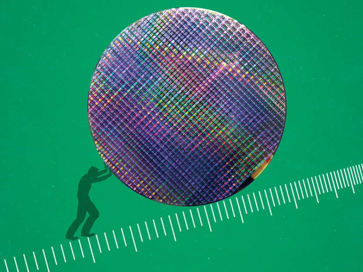
A Better Way to Measure Progress in Semiconductors.jpg


One of the most famous maxims in technology is, of course, Moore’s Law. For more than 55 years, the “Law” has described and predicted the shrinkage of transistors, as denoted by a set of roughly biannual waypoints called technology nodes. Like some physics-based doomsday clock, the node numbers have ticked down relentlessly over the decades as engineers managed to regularly double the number of transistors they could fit into the same patch of silicon. When Gordon Moore first pointed out the trend that carries his name, there was no such thing as a node, and only about 50 transistors could economically be integrated on an IC.....
 
Last edited:
Dan, I feel layering will be the next way to expand capacity of semis as ways to work out the interfacing and the amount of layers that can be formed without interfacing taking up to much overhead. I have listened to presentations by both Micron and Amat in these areas. Any elaboration would be appreciated. Thanks
 
The problem with layering is that it makes the power/current density problems even worse than they are today (and at 5nm they're pretty bad for high-speed circuits). Even with a single layer, for several generations now the circuit area has been shrinking faster than power dissipation per operation, so the power density is going up causing hotspot problems, and the current density has been going up even faster (and metal current capacity has been falling becasue the layers are thinner) so electromigration is even more of an issue.

If you stack layers of circuits both problems get worse still, especially hotspots for the upper layers which are thermally isolated from the (cooled) substrate and EM for the lower layers which are far from the thick metal used for the power grid (or maybe the upper layers if the power grid is buried in the substrate).

So stacking is fine so long as you don't want the stacked circuits to do very much which dissipates power, which kind of removes the point of having them...

(it's OK if the upper layers are mostly "dark silicon" like RAMs or flash, but a huge problem for stacked logic -- which is what people keep proposing)

In a way it's the transistor problem all over again, the real things limiting performance now are getting low-resistance connections (and power) in and out of the transistors because they're so small, not the transistors themselves. Packing more devices into an even smaller area using layers isn't going to work unless the fundamental issues of getting power in and heat out are solved, except for cases where most of the transistors do nothing most of the time...
 
Last edited:
Dan, I feel layering will be the next way to expand capacity of semis as ways to work out the interfacing and the amount of layers that can be formed without interfacing taking up to much overhead. I have listened to presentations by both Micron and Amat in these areas. Any elaboration would be appreciated. Thanks

Gargini seems to have implied similarly:

“Around 2029, we reach the limit of what we can do with lithography,” says Gargini. After that, “the way forward is to stack.... That’s the only way to increase density that we have.”
 
The problem with layering is that it makes the power/current density problems even worse than they are today (and at 5nm they're pretty bad for high-speed circuits). Even with a single layer, for several generations now the circuit area has been shrinking faster than power dissipation per operation, so the power density is going up causing hotspot problems, and the current density has been going up even faster (and metal current capacity has been falling becasue the layers are thinner) so electromigration is even more of an issue.

If you stack layers of circuits both problems get worse still, especially hotspots for the upper layers which are thermally isolated from the (cooled) substrate and EM for the lower layers which are far from the thick metal used for the power grid (or maybe the upper layers if the power grid is buried in the substrate).

So stacking is fine so long as you don't want the stacked circuits to do very much which dissipates power, which kind of removes the point of having them...

(it's OK if the upper layers are mostly "dark silicon" like RAMs or flash, but a huge problem for stacked logic -- which is what people keep proposing)

In a way it's the transistor problem all over again, the real things limiting performance now are getting low-resistance connections (and power) in and out of the transistors because they're so small, not the transistors themselves. Packing more devices into an even smaller area using layers isn't going to work unless the fundamental issues of getting power in and heat out are solved, except for cases where most of the transistors do nothing most of the time...

The 3D XPoint technology that is the basis for Intel's Optane is a great "canary" for 3D thermal issues. Not only is it packed in 3D but the planar density is also high (20 nm hp). And at each x, y, z point there is a heat source that deliberately goes to the melting point (600 C). The heat sinking methods must be applied for sure. So I follow this technology closely with a lot of interest, and some degree of nervousness.
 
Ian makes excellent points. Dennards' Law is long gone but Moore's Trend remains the economic imperative. Now, Dennard was the easy way to scale, but not the only way. There are other ways to control heat, the problem is that they are one-time innovations not repeating rules. So we got better with fins and FDSOI. Now we are getting a step with EUV in particular because it allows more creative fine metals, reducing distance and load. We will get a step with GAA/wires/sheets. Complementary stacking may get us a bump if it brings shorter, smaller loads. Buried/backside power looks like a step. Distributed capacitors (a bit like dead DRAM cells) scattered around the chip or the interposer to shorten the distance that power pulses must travel will likely be a step.

Then there are steps with thermal handling. A socket with 300W dissipation is routine these days, and the next steps are various kinds of liquid cooling, the most aggressive is iBMs etched channels in the backside of the silicon. So we will go from 50W/cm2 silicon to 100W. BTC miners are already there.

The interesting thing is, will 3D be a "step" for improved power? In principle it allows shorter connections and lighter load, at least for the first step of face-to-face with hybrid bonding. But the bond density is at best 1um and more typically 4um, and that is a significant distance in processes today surpassing 80 gates per um2, plus the signal has to travel twice the height of the metal stack and exit through copper which dwarfs the transistors, likely requiring at least some level of long-line drive. This seems too crude to really help with power. Some more subtle layering may be needed, but creating high quality Si crystalline layers is too hot a process to layer over a finished bottom layer of standard CMOS. The DRAM folks only manage their CUA with a combination of heat tolerant circuit process and diligent reduction in the heat of forming the capacitors, but that logic is not as performant as logic chips need.

As for dark silicon, unfortunately that does not exist in all cases. ML chips, a major growth segment needing these leading edge chips, is an example of silicon that never sleeps. For mobile processors and other applications looking mostly for integration at low power, 3D stacking may be more attractive.
 
The 3D XPoint technology that is the basis for Intel's Optane is a great "canary" for 3D thermal issues. Not only is it packed in 3D but the planar density is also high (20 nm hp). And at each x, y, z point there is a heat source that deliberately goes to the melting point (600 C). The heat sinking methods must be applied for sure. So I follow this technology closely with a lot of interest, and some degree of nervousness.
Optane is 99.9% dark silicon. Like soldiers, memory cells endure long stretches of boredom with moments of intense terror. Even the fastest sequential writing will occur long after the heat pulse of a neighbor has faded. Indeed, that local intensity is something they depend upon to get to the transition temperature. The pulse needs to be really fast to minimize the opportunity for energy to dissipate. They can also play tricks with ordering and timing of commands to limit locality if they really need to, in ways that the client devices never notice. Re-ordering writes is easy so long as the controller buffers them while offering a guarantee that they will be written even if power is lost - hold up time for a 10us reordering window needs only a cheap capacitor.
 
Ian makes excellent points. Dennards' Law is long gone but Moore's Trend remains the economic imperative. Now, Dennard was the easy way to scale, but not the only way. There are other ways to control heat, the problem is that they are one-time innovations not repeating rules. So we got better with fins and FDSOI. Now we are getting a step with EUV in particular because it allows more creative fine metals, reducing distance and load. We will get a step with GAA/wires/sheets. Complementary stacking may get us a bump if it brings shorter, smaller loads. Buried/backside power looks like a step. Distributed capacitors (a bit like dead DRAM cells) scattered around the chip or the interposer to shorten the distance that power pulses must travel will likely be a step.

Then there are steps with thermal handling. A socket with 300W dissipation is routine these days, and the next steps are various kinds of liquid cooling, the most aggressive is iBMs etched channels in the backside of the silicon. So we will go from 50W/cm2 silicon to 100W. BTC miners are already there.

The interesting thing is, will 3D be a "step" for improved power? In principle it allows shorter connections and lighter load, at least for the first step of face-to-face with hybrid bonding. But the bond density is at best 1um and more typically 4um, and that is a significant distance in processes today surpassing 80 gates per um2, plus the signal has to travel twice the height of the metal stack and exit through copper which dwarfs the transistors, likely requiring at least some level of long-line drive. This seems too crude to really help with power. Some more subtle layering may be needed, but creating high quality Si crystalline layers is too hot a process to layer over a finished bottom layer of standard CMOS. The DRAM folks only manage their CUA with a combination of heat tolerant circuit process and diligent reduction in the heat of forming the capacitors, but that logic is not as performant as logic chips need.

As for dark silicon, unfortunately that does not exist in all cases. ML chips, a major growth segment needing these leading edge chips, is an example of silicon that never sleeps. For mobile processors and other applications looking mostly for integration at low power, 3D stacking may be more attractive.
If the vertical travel distance can be matched with interposer, then the 2.5D would be chosen instead of actual 3D. This seems inevitable for multiple (hot) processors.
 
Optane is 99.9% dark silicon. Like soldiers, memory cells endure long stretches of boredom with moments of intense terror. Even the fastest sequential writing will occur long after the heat pulse of a neighbor has faded. Indeed, that local intensity is something they depend upon to get to the transition temperature. The pulse needs to be really fast to minimize the opportunity for energy to dissipate. They can also play tricks with ordering and timing of commands to limit locality if they really need to, in ways that the client devices never notice. Re-ordering writes is easy so long as the controller buffers them while offering a guarantee that they will be written even if power is lost - hold up time for a 10us reordering window needs only a cheap capacitor.

With the current in-plane density, it could be pretty close. When one cell is at 600C the neighbor should not get far above 120C. Plus the usual write method is to start by melting (RESET) then crystallize (SET) to the degree needed.
 
I think you all should read Dr. Moore's original paper... not the second one. the second one had become so popular but actually the first one includes the most critical message. In short, his view was that cost will justify the products and if the same product that function is the same, the least costly product will sell, and hence the company that manufacture such products will win. This hasn't actually changed at all, even if you apply the same argument in world war II actually(pls compare German heavy tank King Tiger II vs. US Sharman tank). and so is the same for Auto industry, and Ford is the very first company who did exactly what Moore's first paper was practically pointed out. This is simply because of more profit margin can be obtained. And integrating parts will make it possible as a simple solution, back then, to do that. Now, scaling is coming down significantly slower than before, but that doesn't necessarily indicate there's no way to reduce cost of manufacturing. So, as long as integration continues, product cost will be reduced, and hence small company may face serious issue competing a big ones, as the cost merit is not as that big, while I can say a bit company has a lot more structural, hierarchical and/or bureaucratic issues, so it' going to be a question. But in essence, I don't think nothing will change in attempt of reducing cost structures anyway, even now, just like in the old days. So, nothing has changed since mass production era had started since Ford.
 
I've argued over the years that it will be economics that ultimately kill Moore's law, not technological limitations - although the two are interlinked. Fewer and fewer products will make sense to migrate to the next node given the cost, so there will only be a small segment of the semiconductor market where there is any real reason to shrink down to say 1.5nm, and with the fabs getting more and more expensive will it make sense to even build a fab to address a limited market? I think we'll see different innovations, in area like packaging, chiplets, interconnects, ect, that will bring incremental performance and features, but we won't get the density and speed improvements.
 
Back
Top