
triceratops24
New member
[Exclusive] Samsung Electronics changes the process name of ‘2nd generation 3-nano’ to ‘2-nano’
Announcement to partners and customers early this year... mass production possible as early as the end of this yearSemiconductor/Display Entered: 2024/03/05 15:03 Modified: 2024/03/05 22:21
Samsung Electronics decided to change the name of its foundry (semiconductor consignment production) ‘2nd generation 3 nanometer (nm)’ process to ‘2 nano’. In other words, the plan is to call the 2nd generation 3-nano process, which was targeted for mass production within this year, as 2-nano process.
According to the semiconductor industry on the 5th, Samsung Electronics announced to its customers and partners from the beginning of this year that it would change the name of its 2nd generation 3-nano process to 2-nano. There has been talk in the industry regarding Samsung Electronics' 2-nano name change since the end of last year, but the name change has recently been officially confirmed.
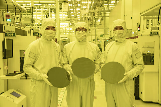
On June 30, 2022, Samsung Electronics Foundry Division (from left) Executive Director Won-cheol Won, Vice President Ja-heum Koo, and Executive Director Sang-beom Kang are showing a 3-nano wafer at the 3-nano mass production line at the Hwaseong Campus. (Photo = Samsung Electronics)
An official in the fabless industry said, "We have been notified by Samsung Electronics that the 2nd generation 3-nano technology will be changed to 2-nano technology," adding, "The contract signed with the Samsung Electronics foundry last year for the 2nd generation 3-nano device was also renamed to 2-nano technology, and the contract was recently rewritten. "he said.
It is understood that Samsung Electronics' recent order for a 2-nano process AI accelerator chip from Japanese AI startup PFN (Preferred Networks) is in fact a second-generation 3-nano process. The chip is targeted for mass production in 2025.
Samsung Electronics began mass production of 3-nano chips based on the gate-all-around (GAA) process for the first time in the world at the end of June 2022, and plans to mass produce the second-generation 3-nano process this year and the 2-nano process in 2025. As the name has been integrated into the 2-nano process, Samsung Electronics is expected to begin mass production of 2-nano chips as early as the second half of this year.
An official in the semiconductor industry said, "Samsung Electronics' second-generation 3-nano (2-nano) process design kit (PDK) has already been released, so if we go too far in mass producing it this year, it will be enough." He added, "The foundry will begin mass production at the request of customers." “It’s not something you can say you want to do,” he said.
There is an industry interpretation that Samsung Electronics' process name change could be advantageous in terms of foundry marketing. It is also a recent PR trend in the foundry industry.
Previously, when Samsung Electronics moved from the 7-nano process to the 5-nano process in 2020, the name of the second-generation 7-nano process was changed to 5-nano. Samsung Electronics' 7nm process was the world's first in 2019 to use extreme ultraviolet (EUV) technology. As a result of making this more stable, the transistor size was reduced, and the name of the 2nd generation 7-nano was changed to 5-nano.
An industry insider said, "Samsung Electronics' 3-nano process was the first GAA process, but it appears that the name was changed to 2-nano as the transistor size was reduced through optimization." He added, "This may be marketing or promotion, but on the other hand, it is the result of the advancement work. “It can be seen as one of them,” he explained.
Last edited by a moderator:
