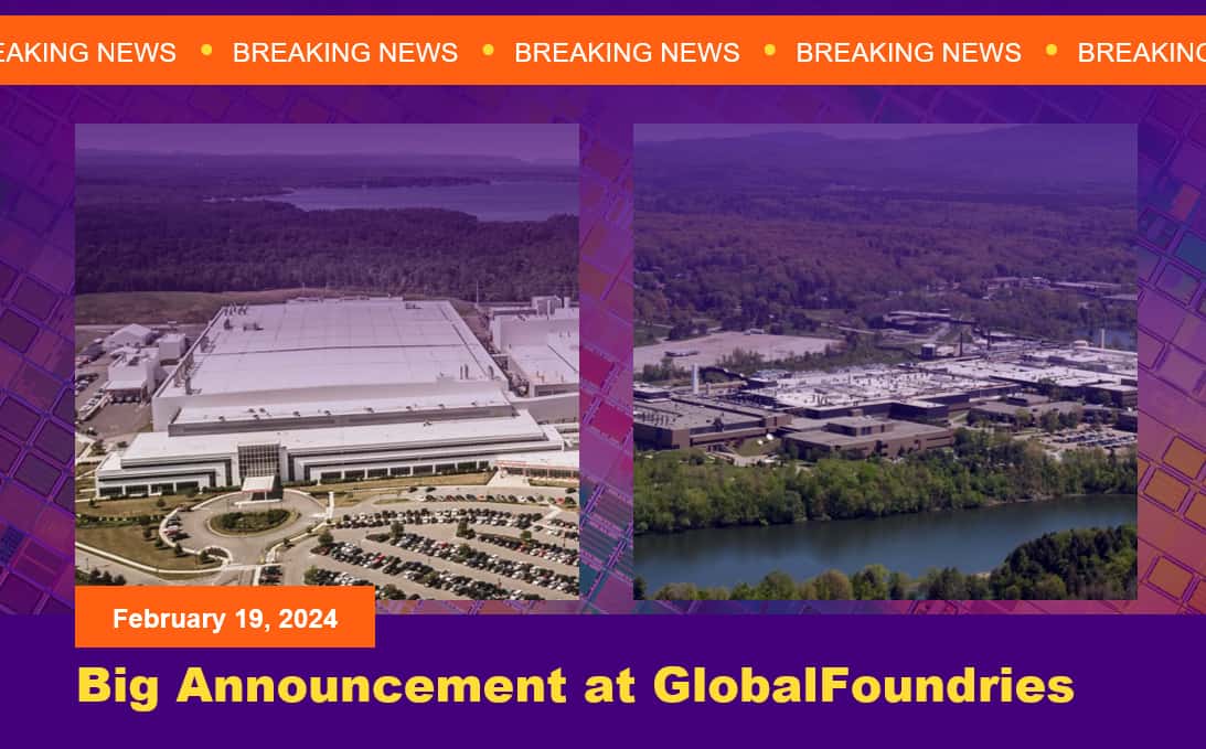
Monday, February 19, 2024
Biden-Harris Administration Announces Preliminary Terms with GlobalFoundries to Strengthen Domestic Legacy Chip Supply for U.S. Auto and Defense Industries
U.S. Department of Commerce Outlines $1.5 Billion in Potential Funding to Support Multiple Projects in New York and Vermont and Create Approximately 10,500 Construction and Manufacturing Jobs
Today, the Biden-Harris Administration announced that the U.S. Department of Commerce and GlobalFoundries (GF) have signed a non-binding preliminary memorandum of terms (PMT) to provide approximately $1.5 billion in direct funding under the CHIPS and Science Act to strengthen U.S. domestic supply chain resilience, bolster U.S. competitiveness in current-generation and mature-node (C&M) semiconductor production, and support economic and national security capabilities. The proposed funding would support a new state-of-the-art facility, significant capacity expansion, and the modernization of GF’s U.S. manufacturing sites in New York and Vermont, which produce essential automotive, communications, and defense semiconductor technologies.
President Biden signed the bipartisan CHIPS and Science Act to strengthen U.S. supply chains, create good-paying jobs, and advance U.S. economic and national security. Today’s announcement is the third PMT announcement the Department of Commerce has made under the CHIPS and Science Act.
GF chips are fundamental to everyday applications that impact all Americans, from blind spot detection and collision warnings in cars, to smartphones and electric vehicles that last longer between charges, to secure and reliable Wi-Fi and cellular connections. Currently, there are only four companies outside of China that provide current and mature foundry capabilities at the scale of GF – and GF is the only one of those companies that is headquartered in the United States. Shortages of some of these semiconductors caused major disruptions during the COVID-19 pandemic, resulting in a particularly acute impact on the availability and price of a broad range of goods for Americans, as well as the shutdown of automobile manufacturing sites. Part of the proposed funding is expected to support expanding the facility that houses a dedicated capacity corridor for General Motors, with whom GF entered into a strategic long-term supply agreement last year.
“Semiconductors are the brain of modern technology. While they are no larger than a fingernail and no thicker than a piece of paper, they are essential to every electronic device that we currently use – from computers and televisions to cars and washing machines. Thanks to our Administration’s CHIPS and Science Act, we are announcing the Department of Commerce’s preliminary agreement with GlobalFoundries, which will award approximately $1.5 billion to expand domestic production of semiconductors, strengthen U.S. supply chains, and create thousands of good paying jobs right here in America,” said
Vice President Kamala Harris.
“President Biden and I continue to be fully committed to growing our economy and creating opportunity in every part of America. Today’s announcement is another way in which we are delivering on that commitment in New York, Vermont, and communities throughout the country.”
“Semiconductors are in everything from our cellphones, to refrigerators, to cars, and our most advanced weapons systems, and access to them carries important economic and national security implications. It was the shortages of semiconductors during the COVID-19 pandemic that raised prices for consumers and led to the shutdown of automobile manufacturing sites across the country,” said
Secretary of Commerce Gina Raimondo.
“Thanks to President Biden’s CHIPS and Science Act, we’re working to onshore these critical technologies in order to bolster the supply of domestic chips that are essential to manufacturing cars, electronics, and national defense systems in New York, Vermont, and states across the country.”
“The CHIPS and Science Act set out to make the United States a leader in semiconductor R&D and manufacturing, and with this proposed CHIPS funding, GlobalFoundries could help realize this vision by modernizing and building new chip fabrication facilities to increase its capacity to make current-generation and mature-node chips in the United States while creating thousands of good jobs in New York and Vermont,” said
Under Secretary of Commerce for Standards and Technology and NIST Director Laurie E. Locascio.
“By investing in domestic manufacturing capabilities, CHIPS for America is helping secure a stable domestic supply of chips that are found in everything from home electronics to advanced aerospace systems.”
"GF is proud to announce this proposed funding from the Department of Commerce and appreciates the collaboration of the CHIPS Office throughout this process. These proposed investments, along with the investment tax credit (ITC) for semiconductor manufacturing, are central to the next chapter of the GlobalFoundries story and our industry. They would also play an important role in making the U.S. semiconductor ecosystem more globally competitive and resilient," said
Dr. Thomas Caulfield, president and CEO of GF. "With new onshore capacity and technology on the horizon, as an industry we now need to turn our attention to increasing the demand for U.S.-made chips, and to growing our talented U.S. semiconductor workforce."
The proposed expansion of GF is expected to help advance U.S. economic and national security by increasing capacity, strengthening supply chain resilience, and onshoring technologies in the U.S. for the first time that are important to our defense and intelligence communities. With multiple facilities that are designated as Trusted Foundries by the Department of Defense, GF has a long history of supporting the U.S. military and this proposed funding is expected to strengthen those ties. The Department of Defense relies on GF chips for national defense uses including satellite and space communications. GF chips also support broader U.S. technological leadership and discovery, such as the James Webb Telescope and the International Space Station.
The approximately $1.5 billion in proposed CHIPS funding would be split across three projects:
Malta, New York – New State-of-the-Art 300 mm Fab: The construction of a new, large-scale 300 mm fabrication facility that is expected to produce high value technologies not currently available in the U.S. The new facility is intended to leverage existing infrastructure to expedite the path from construction to production.
Malta, New York – Capacity Expansion for Automotive: The proposed expansion of the existing Malta, New York fabrication facility, which includes a strategic agreement with General Motors, to secure a dedicated supply of essential semiconductor technologies. This project would also support America’s economic and national security by expanding domestic capacity for semiconductors that are used in the U.S. critical infrastructure base. This expansion, combined with the new 300 mm fabrication facility, is expected to triple the existing capacity of the Malta campus over the next 10+ years. These two projects are expected to increase wafer production to 1 million per year once all phases are complete.
Burlington, Vermont – Fab Revitalization: The revitalization of an existing fabrication facility in Burlington, Vermont, to commercialize new 200 mm technologies, creating the first U.S. facility capable of high-volume manufacturing of next-generation Gallium Nitride on Silicon for use in electric vehicles, power grid, 5G and 6G smartphones, and other critical technologies. The site will apply industry-leading sustainability practices, including the use of 100% carbon-free neutral energy and the development of an onsite solar system to supply up to 9% of the site’s annual energy.
The proposed projects would create approximately 1,500 manufacturing jobs and approximately 9,000 construction jobs over the next 10 years. The PMT also proposes approximately $10 million in dedicated workforce development funding for GF to work with local workforce, education, training, and community-based organizations to provide GF with the facilities and construction talent they need now and in the future. GF also continues to build upon its GF Maintenance Technician Apprenticeship Program, which is the first U.S. registered semiconductor apprenticeship program and graduated its first apprentices in 2022. In recognizing the critical importance of child care for its operations, the company will not only continue to provide its $1,000 annual subsidy and child care support concierge service to its growing facility workforce but also extend these benefits to its construction workers. The company will be operating under an existing Project Labor Agreement (PLA) in New York and is in the process of establishing a PLA in Vermont for the purposes of this project.
In addition to potential direct funding, the CHIPS Program Office would make approximately $1.6 billion in loans available to GF under the PMT. The total potential public and private investment for the combined projects would be approximately $12.5 billion.
As explained in the Department’s first
Notice of Funding Opportunity, the Department may offer applicants a PMT on a non-binding basis after satisfactory completion of the merit review of a full application. The PMT outlines key terms for a CHIPS incentives award, including the amount and form of the award. After the PMT is signed, the Department begins a comprehensive due diligence process on the proposed project and other information contained in the application. After satisfactory completion of the due diligence phase, the Department may enter into final award documents with the applicant. Terms of the final award documents are subject to negotiations with the applicant and may differ from the terms of the PMT.
About CHIPS for America
The Department has received more than 600 statements of interest, more than 160 pre-applications and full applications for NOFO 1, and more than 160 small supplier concept plans for NOFO 2. The Department is continuing to conduct rigorous evaluation of applications to determine which projects will advance U.S. national and economic security, attract more private capital, and deliver other economic benefits to the country. The announcement with GlobalFoundries is the third PMT announcement the Department of Commerce has made under the CHIPS and Science Act, with additional PMT announcements expected to follow throughout 2024.
CHIPS for America is part of President Biden’s economic plan to invest in America, stimulate private sector investment, create good-paying jobs, make more in the United States, and revitalize communities left behind. CHIPS for America includes the CHIPS Program Office, responsible for manufacturing incentives, and the CHIPS Research and Development Office, responsible for R&D programs, that both sit within the National Institute of Standards and Technology (NIST) at the Department of Commerce. NIST promotes U.S. innovation and industrial competitiveness by advancing measurement science, standards, and technology in ways that enhance economic security and improve our quality of life. NIST is uniquely positioned to successfully administer the CHIPS for America program because of the bureau’s strong relationships with U.S. industries, its deep understanding of the semiconductor ecosystem, and its reputation as fair and trusted. Visit
https://www.chips.gov to learn more.
GlobalFoundries Contacts
GlobalFoundries Media Relations: Erica McGill at
erica.mcgill@gf.com
GlobalFoundries NY Community Contact: Julie Moynehan at
julie.moynehan@gf.com
GlobalFoundries VT Community Contact: Gina DeRossi at
gina.derossi@gf.com
 techovedas.com


