A High NA EUV tool is seen before the attachment of its top module as it is assembled at ASML’s headquarters in Veldhoven, Netherlands, November 14, 2023. ASML/Michel de Heer/Handout via REUTERS© Thomson Reuters
By Toby Sterling
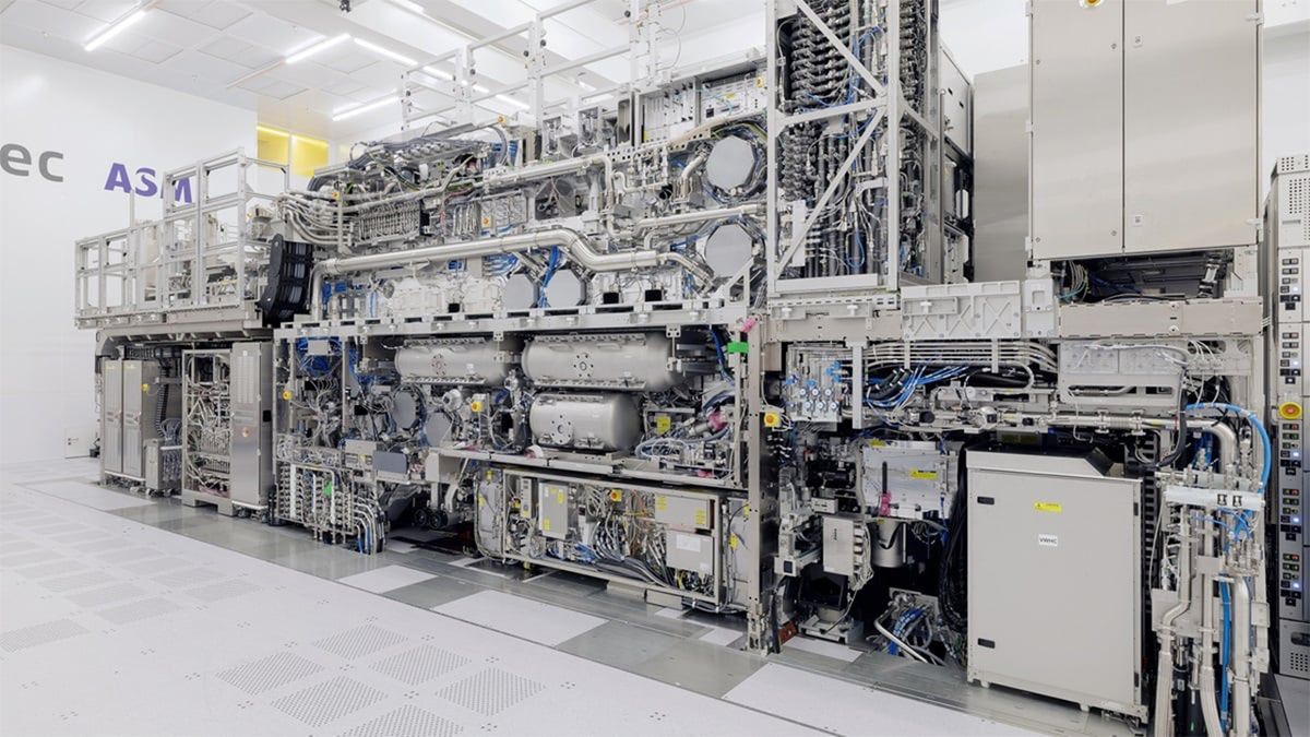
VELDHOVEN, Netherlands (Reuters) - Chip toolmaking giant ASML said on Friday it was gearing up production of its new $350 million "High NA EUV" machine, a device the size of a double decker bus central to its bid to keep its lead in a $125 billion market.
The machine, which went on display for the first time on Friday in the Dutch headquarters of Europe's largest tech company by market value, is aimed at Intel and other makers of the highest-end semiconductors.
ASML said it was expecting to ship "a number" of them this year, and there was still work to do on customising and installation.
"We keep engineering and developing and there's a lot of work to be done to calibrate it and make sure it fits into the manufacturing system," ASML spokesperson Monique Mols said. "There's also a steep learning curve for us and our customers."

Workers at Carl Zeiss ZMT are seen outside giant vacuum chambers where optical systems for ASML’s new High NA EUV tool are tested. ASML is rolling out its newest product line, High NA EUV lithography tools, which cost more than $350 million each and will be used by leading semiconductor manufacturers to help make new generations of smaller and better computer chips in Oberkochen, Germany, December 12, 2023. ASML/ZEISS/Handout via REUTERS© Thomson Reuters
ASML is the only maker of a key technology - extreme ultraviolet (EUV) photolithography - needed to manufacture the most advanced chips.
High NA EUV is the next generation of that technology. But analysts said it was an open question how many customers are ready to switch over to the high-cost devices.
Customers could choose to wait and squeeze more out of existing tools. Koch's own calculations suggested it would only become cost effective to switch over from the older technology around 2030-2031.
ASML CEO Peter Wennink told Reuters in January analysts may be underestimating the technology.
"Everything that we're currently seeing in the discussion with our customers is that High NA is cheaper," he said in an interview.
Greet Storms, head of ASML's High NA product management, said on Friday an inflection point is coming around 2026-2027.
"This is the point clients will take it into volume production," she told reporters.
Intel has already taken delivery of one pilot device, and said it plans to start production next year, without giving details on the scale of the operation.
TSMC and Samsung have said they intend to use the tool but have not specified when.
ASML says it has taken between 10 and 20 orders to date - including pilot devices for memory specialists SK Hynix and Micron - and is building capacity to be able to deliver 20 annually by 2028.
None of them will go to China, ASML's second-largest market last year, as the United States seeks to curb exports of cutting-edge technology there and stymie Beijing's semiconductor ambitions.
Last month though, the company, considered a bellwether for the chip industry, reported a robust order book which soothed investors' concerns that limits on China would hurt its performance.
A quick take-up of the tool would boost ASML's sales and margins and could extend its dominant position in the market for lithography systems, machines that use light to help trace out patterns on silicon wafers that will eventually become the circuitry of computer chips.
It says the High NA tool will let chipmakers shrink the size of the smallest features on their chips by up to 40%, allowing density of transistors to nearly triple.
ASML competes with Nikon and Canon of Japan to make the lithography machines used to make relatively older generations of chips.
But in the late 2010s, the Dutch firm became the first and only company to market a lithography tool using EUV, or 13.5 nanometre wavelength light.
Both the original and High NA machine create EUV light by vaporizing droplets of tin with twin laser pulses 50,000 times a second.
ASML says the High NA machine's biggest change is a larger optical system consisting of irregularly shaped mirrors, made by Carl Zeiss, polished so smooth they must be kept in a vacuum. They collect and focus more light than their predecessors - High NA stands for high numerical aperture - which is what the company says leads to better resolution.