You are currently viewing SemiWiki as a guest which gives you limited access to the site. To view blog comments and experience other SemiWiki features you must be a registered member. Registration is fast, simple, and absolutely free so please, join our community today!
Samsung's upcoming in-house SoCs, the Exynos 2500 and Exynos W940, fabricated on SF's 3nm GAA process node, may be delayed. The foundry faced issues with
Samsung's upcoming in-house SoCs, the Exynos 2500 and Exynos W940, fabricated on SF's 3nm GAA process node, may be delayed. The foundry faced issues with
Yes. It was the same with Samsung 10nm. When they announced HVM yield was single digit so they only sold good die to QCOM.
As far as Samsung 3nm design wins there was one in China, a crypto currency ASIC but that was it. After the 10nm, 5/4nm, and now 3nm yield fiascos it is hard to believe anyone will trust Samsung Foundry with their products.
I wasn't exactly expecting the world, but I feel like 0% is just way too low to be believable (even if you ignore the SK press's dubious reporting history). The SF3E crypto chip may have been like 20mm^2, lacking any SRAM or analog devices, but they had at least a some working dies for the customer and later techinsights to get their hands on. IF the rumors are true and the plan was a smartwatch launch in late summer/early autumn, it is hard to imagine a similarly sized more complex SOC on SF3 has a defect density that is so much worse than SF3E years later that they are getting 0% die yield. I guess we will know come Aug/Sept when they normally do watch launches. Even if the defect density isn't great, I would assume they can scrounge up enough dies to launch something anything!? If all we see is more SF4, I think Cannonlake might have just been supplanted. 1st gen GAA from Samsung was originally scheduled for risk production in 2021. If we need to wait for 2025 that is somehow even worse than the 3 years of delays intel had for 10nm...
Samsung's upcoming in-house SoCs, the Exynos 2500 and Exynos W940, fabricated on SF's 3nm GAA process node, may be delayed. The foundry faced issues with
Some inputs:
a. If it was real product tapeout, it is questionable. Typically, before launching engineering full run, you might test design in test vehicle or MPW wafer first for design debugging.
NTO DOA (0 yield) is disastrous, but could be easy to find out the problems comparing with baseline of single digit yield.
b. Low yield is troublesome. Assumed you get yield 30% with GDPW=500 and with no reliability correlation with lower yield wafers, then you get 150 dies per wafer. To prepare new mobile phone launch, we might need at least 10-15kk chips/month, which means to produce ~70-100k wafers output/month. If yield goes 60% or above, then the capacity needed is half of that and cost is less than half also. For 3nm using EUV tools, you need more than 30 EUV tools be ready in production of 70k wafer capacity soon.
It is easy to "Talk the Talk". Go for all Engineers for advanced node production.
Are Samsung's issues likely to also torpedo other foundries' ribbonFETs at scale, is the next question. Generally everyone expects a technology to improve yield in the foundry, not so much the lab, so if that improvement is the problem then others may be in for a surprise.
I would expect the competitors are trying to find every scrap of intelligence.
Discover Samsung's groundbreaking 3nm chip and its application in ASIC miners. Learn about its advantages, energy efficiency, and potential impact on the cryptocurrency mining industry.
cryptoage.com
This is not the most efficient chip. BitMain makes one 20% more efficient, claiming it is done on TSMC N7. That is a curious result for 3 vs. 7.
Are Samsung's issues likely to also torpedo other foundries' ribbonFETs at scale, is the next question. Generally everyone expects a technology to improve yield in the foundry, not so much the lab, so if that improvement is the problem then others may be in for a surprise.
I would expect the competitors are trying to find every scrap of intelligence.
It is good question. Intel Pat Gelsinger said they will complete 5 nodes in 4 years by 2024 including RibbonFET 20A/18A be ready in 2024, but TSMC said N2 will be ready in 2025 and on track now. What I know is either 20A/18A or TSMC N2 are not pushing DR but only have device architecture change comparing with previous FinFET node.
Although intel pushes out Hi NA EUV adoption in 18A due to the timing of Hi NA HVM readiness, I just wondered why intel planned Hi NA EUV in their 18A at beginning.
Overall I call BS on that blog. Random rumor with no indication of source and no other reports except echoes of this one. Other sites with a track record have reported rising yields months ago. Looks like a desperate blog.
Although intel pushes out Hi NA EUV adoption in 18A due to the timing of Hi NA HVM readiness, I just wondered why intel planned Hi NA EUV in their 18A at beginning.
I suspect that wiring density is the killer app for Hi NA, more so than devices. This is because the devices are susceptible to very regular placement and orientation, and cuts on the ribbons will not be dense, so ordinary EUV or even quad pitch multiplier 193i could work for the ribbon formation and device separation. But wiring patterns are dense so if they want to get jiggy with layers 0 and 1 then Hi NA may be up to bat.
Samsung's upcoming in-house SoCs, the Exynos 2500 and Exynos W940, fabricated on SF's 3nm GAA process node, may be delayed. The foundry faced issues with
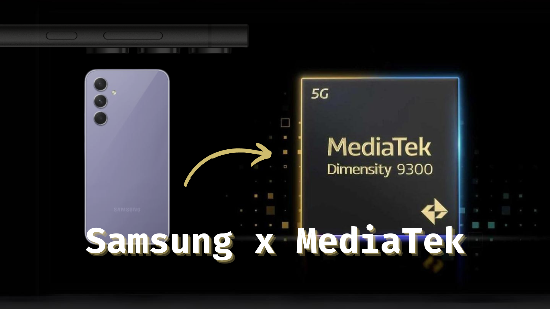
The race for the best smartphone SoC will unquestionably intensify by the end of this year as all major chipset manufacturers transition to 3nm. The
appuals.com
"Despite the competition being fierce, the story on the lower end of the spectrum is completely different. There is a possibility that Samsung may choose to incorporate MediaTek SoCs in its budget line of smartphones instead of it’s own in-house Exynos chipsets."
This a not a correct observation.
Samsung has been using MediaTek chips for a long time on its low-end or midrange smartphones.
I suspect that wiring density is the killer app for Hi NA, more so than devices. This is because the devices are susceptible to very regular placement and orientation, and cuts on the ribbons will not be dense, so ordinary EUV or even quad pitch multiplier 193i could work for the ribbon formation and device separation. But wiring patterns are dense so if they want to get jiggy with layers 0 and 1 then Hi NA may be up to bat.
The author's credentials are lacking, to put it mildly...
ABOUT THE AUTHOR
Muhammad Qasim
Qasim's deep love for technology and gaming drives him to not only stay up-to-date on the latest developments but also to share his informed perspectives with others through his writing. Whether through this or other endeavors, he is committed to sharing his expertise and making a meaningful contribution to the world of tech and gaming.
Overall I call BS on that blog. Random rumor with no indication of source and no other reports except echoes of this one. Other sites with a track record have reported rising yields months ago. Looks like a desperate blog.
The race for the best smartphone SoC will unquestionably intensify by the end of this year as all major chipset manufacturers transition to 3nm. The
appuals.com
"Despite the competition being fierce, the story on the lower end of the spectrum is completely different. There is a possibility that Samsung may choose to incorporate MediaTek SoCs in its budget line of smartphones instead of it’s own in-house Exynos chipsets."
This a not a correct observation.
Samsung has been using MediaTek chips for a long time on its low-end or midrange smartphones.
Samsung has historically been only making a flagship SoC model only. Bin rejects - > crusher
Now they added a smaller SoC, with less bells, and whistles to the lineup, but they still follow same conservative binning. MediaTek on the other hand will cut wafers into up to 4 models based on binning. That is generally kept under wraps by their marketing. The chip marketing name may be Helio P90, but that may be 2-3 different models really sold under that name.
MediaTek's economy for low-end is inherently better.
News seems busted. Actually the news doesn't look true to me. Samsung have been maunfacturing mining ASICs for a year, so It's hard to believe that their Galaxy Watch(Exynos W940, small chip) is running 0% yield. Maybe some insider saw failed experiement in certain lot?
News seems busted. Actually the news doesn't look true to me. Samsung have been maunfacturing mining ASICs for a year, so It's hard to believe that their Galaxy Watch(Exynos W940, small chip) is running 0% yield. Maybe some insider saw failed experiement in certain lot?
good input. It is not unheard of for a product to zero on a process due to patterning or parametric issue.
I think it is more likely, based on history:
1) Samsung yields are very low. They overstart wafers to make up for it. This has been confirmed on previous processes and GAA is VERY hard.
2) If they are zero on a new product, they must have pilot lots, and they must have a backup plan.
Samsung will survive with backup plans and overstarts and deals with customers. As Dan mentioned, this is really not a new challenge for Samsung. Samsung loves the PR of bleeding edge processes and lives with the inconsistency and churn.
The parametric/defect yield meanings are too ambiguous. We usually talk about CP yield or FT yield, typically will not be wafer outgoing WAT yield. Some failure could be related to bad process control not related to particles, and some could be related which seems meet your defect yield. It will not be the yield reported using inspection tools in WIP which are not possible to scan whole wafers in all lots. It is not economically feasible.


 appuals.com
 www.breakinglatest.news