We live in very interesting times, you can wear an Android watch from Samsung that uses 14 nm FinFET technology, attend the 52nd DAC conference in June to learn about EDA and IP vendors supporting FinFET, and read about research work for new devices down to 5 nm. TCAD is that critical software technology that enables the development of new devices at 10 nm, 7 nm and even 5 nm. To get an update on what Synopsys has to offer in the TCAD space I spoke by phone with Tom Ferry last week, we both worked at a company called CrossCheck back in the 90’s. According to data from EDAC we learn that Synopsys is #1 in TCAD software.
Related – EDA Mergers and Acquisitions Wiki
Synopsys categorizes TCAD software as Silicon Manufacturing and places it into three segments:
- Device and Process R&D
- Mask Creation
- Yield Management
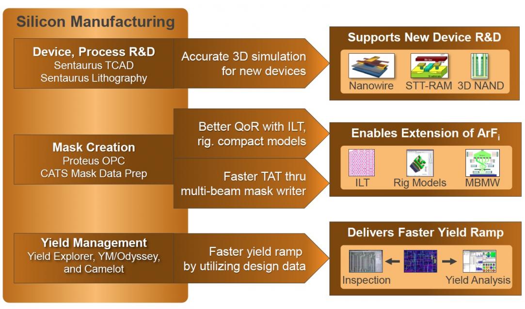
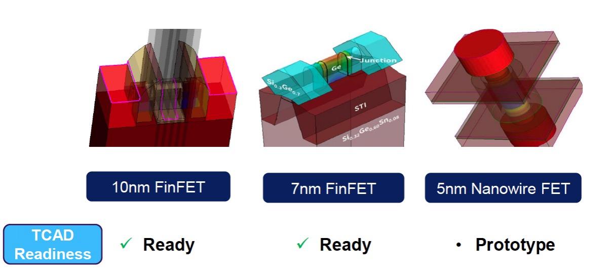
Device and process engineers have used tools like Sentaurus TCAD and Sentaurus Lithography to define and optimize their 10 nm and 7 nm FinFET technologies, while at 5 nm the Nanowire FinFET is still at a prototype stage.
For my MacBook Pro laptop I replaced the hard drive with an SSD from Samsung and it uses a planar NAND structure, while the newest Samsung SSD use a 3D NAND structure. Both the planar NAND and 3D NAND structures are supported in Sentaurus today, while emerging technologies like ReRAM (Resistive RAM) and STT-RAM (Spin Torque Transistor RAM) are in a prototype stage.
Related – 25 Years of SNUG; 50 Years of Moore’s Law
IMEC is a leading research consortium and they’re collaborating with Synopsys to deliver a version of Sentaurus to enable design and optimization of 5 nm technology and smaller nodes.
Using 193 nm light sources to resolve feature sizes for smaller node sizes is a huge challenge that requires OPC (Optical Proximity Correction) and RET (Resolution Enhancement Technology) to print reliable features while not filling up your disks with mask data. Run time is the other bottleneck for running these OPC and RET tools. There are two approaches from Synopsys that meet these litho challenges using the Proteus software:
- Proteus rigorous compact OPC models
- Proteus Inverse Lithography Technology (ILT)
A rigorous model is based on physical parameters, which is essential to predict the behavior of new devices, instead of using empirical parameters. ILT is a technology started some 10 years ago, however at first the run times were 10X slower than OPC. The Synopsys approach is to selectively target where ILT gets used to the most critical design areas, providing QOR improvements with a smaller mask cost increase. This ILT technology came from the acquisition of Luminescent back in 2012. The Proteus ILT approach is being qualified for 10 nm mask flows now. Here’s where ILT fits into the mask synthesis flow:
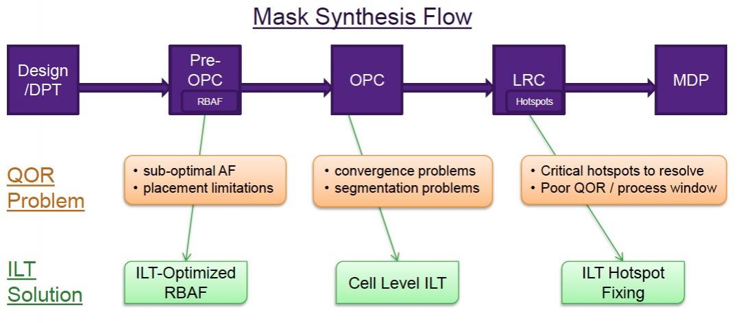
To get the run times lower you use Proteus across a network of CPUs, it could even be thousands. Running a verification tool like Proteus LRC will find a hotspot, then the ILT will fix each hotspot locally so that you don’t have to run OPC and RET again on the whole chip.
Related – FinFET Design Enablement
The time required to write a mask is increasing, however it must be kept under a threshold for equipment reliability reasons.
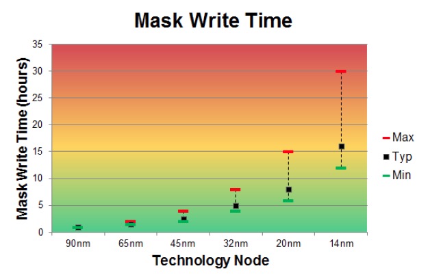
The Proteus to CATS flow happens in parallel to help shorten this mask writing time. Another speed improvement comes from using the multi-beam mask writer from IMS, now supported by CATS.
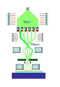
There’s even a new mask writer machine from NuFlare called the EBM 8000 that uses variable-shaped beam equipment to reduce write times by 1.5X to 2.0X.
Once a new IC goes into silicon production the biggest question becomes one of yield, and discovering why a specific design has low yield. Synopsys has software called Excalibur running on inspection machines, locating failures in process that are design dependent. Outside of the fab test engineers can run the Yield Explorerand Camelot tools to perform failure analysis on an IC and then pinpoint the failure on a SEM (Scanning Electron Microscope). Inside of a fab they use the Odyssey software as a defect management system.
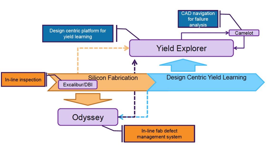
What makes Synopsys different in yield improvement is that they have connections across all three domains: Design, Fab and Test.
Conclusion
Synopsys has a strong history in the TCAD software business and their Sentaurus tool is used for 10 nm, 7 nm and 5 nm devices enabling Moore’s law to continue. Process window requirements are met with the Proteus ILT and modeling approach. Mask write times can be met with CATS fracturing. Give your Synopsys rep a call to find out more details, or visit at one of the conferences:
Share this post via:


Comments
There are no comments yet.
You must register or log in to view/post comments.