
As analog and mixed-signal designs become increasingly complex, parasitic effects dominate both design time and cost, consuming 30–50% of engineers’ effort in debugging and reanalyzing circuits. Addressing these multiphysics effects requires early verification strategies and reliable simulation solutions. Modern verification must extend beyond traditional RC parasitics to encompass inductance, RF interactions, voltage drop, RDS(on) effects, thermal behavior, signal integrity, photonics, and electrostatic discharge (ESD).
Synopsys recently hosted a webinar on ESD verification for full-chip and multi-die designs using its PathFinder-SC platform. The session was presented by Peter Tsai, Product Manager; Marc Swinnen, Product Marketing Manager; and John Alwyn, Product Specialist. It provided a detailed look at PathFinder-SC’s capabilities in addressing modern ESD verification challenges, highlighting workflows for early-stage validation, full-chip and multi-die simulation, and layout-driven debugging. The session emphasized effective protection circuits, bump-to-bump, bump-to-clamp and clamp-to-clamp discharge paths, and adherence to foundry-certified thresholds for voltage, current, and electromigration limits.
Synopsys PathFinder-SC Overview
PathFinder-SC enables early ESD verification through cell-based modeling of discharge circuits derived from GDS, OASIS, DEF, and LEF data. This approach allows potential reliability issues to be identified well before full layout completion. Its scalable architecture, powered by the Seascape distributed computing platform, supports simulations of full-chip and multi-die designs with billions of nodes.
By leveraging RedHawk-SC’s certified extraction and electromigration engines, PathFinder-SC ensures that effective resistance and current density checks comply with foundry guidelines. This guarantees that discharge paths, metal routing, and protection circuits can safely handle ESD currents. Layout-driven debugging allows engineers to trace shortest-path resistances, visualize current density flows, and pinpoint potential failure points.
Multi-scenario simulations that include variations in bump placement, clamp types, and extraction corners help optimize design robustness. PathFinder-SC also extends verification from the die to the package and board level, incorporating package netlists and compact impedance models to ensure end-to-end reliability.
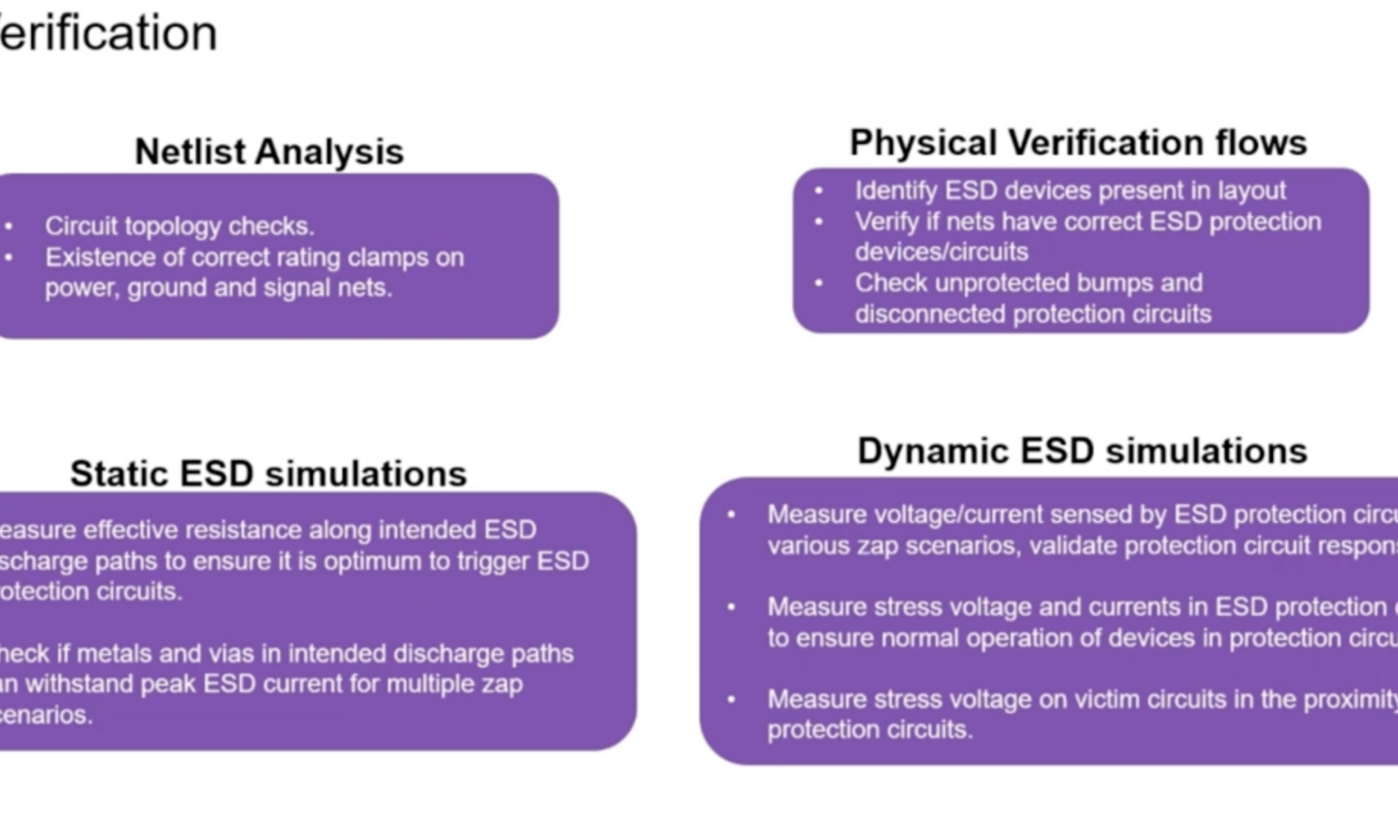
Technical Capabilities and Workflows
PathFinder-SC supports static ESD simulations, including effective resistance and current density checks along intended discharge paths. It verifies protection circuits such as primary and secondary diodes, clamps, and cross-domain devices, ensuring that ESD currents safely exit through the nearest bump without damaging functional circuits. When discharge paths are poorly routed or have insufficient metalization, unintended paths may form, potentially causing latent device damage. PathFinder-SC detects these weaknesses early, enabling designers to optimize layouts before fabrication.
Simulation workflows include design netlist analysis, physical verification, static resistance and current density simulations, and dynamic simulations. Using schematic and layout checks, PathFinder-SC identifies ESD devices, verifies connections, and ensures compliance with foundry guidelines. Static simulations measure effective resistance and current density along partial or full discharge paths, while dynamic simulations assess peak stress voltages and currents in protection circuits. These analyses enable robust verification of bump-to-bump, bump-to-clamp, and clamp-to-clamp paths, including multi-die interposer connections.

Distributed processing via Seascape allows large designs to be simulated efficiently. Tasks such as geometry processing, resistance extraction, zap simulations, and result aggregation are parallelized across hundreds of CPU cores or cloud workers. PathFinder-SC can handle designs with hundreds of thousands of bumps, tens of thousands of protection devices, and multiple dies, completing workflows in hours rather than days. Sensitivity analysis and shortest-path resistance tracing allow engineers to pinpoint high-resistance segments and electromigration hotspots for targeted optimization.
The tool’s view-based architecture supports simulation of multiple variations in bump placement, clamp types, and extraction corners. Each view executes workflows such as RC extraction, clamp identification, and zap simulations, with results stored in a distributed database for analysis. Users can query the database, visualize current density and electromigration maps, and browse resistance check results for full-chip or multi-die designs. Compact impedance modeling and detailed standard parasitic format (DSPF) stitching allow transient simulations of ESD events, linking die-level and package-level effects.


Performance Insights
Performance metrics shared during the webinar demonstrated PathFinder-SC’s ability to handle very large designs efficiently. Full-chip SoCs and multi-die stacks with millions of nodes, tens of thousands of clamps, and hundreds of thousands of bumps were simulated using distributed workers.
For example, a multi-die 3DIC design with 168,000 protection diodes and 144 clamps completed clamp-to-clamp and bump-to-clamp resistance checks in under 14 hours using 80 CPUs. Current density simulations for a 5nm SoC with around 163,000 PG bumps finished in about 37 hours using 50 CPUs. A very large interposer layout covering 24 cm × 18 cm, with over 500,000 nets and 163 million geometry shapes, completed extraction and design modeling in 47 hours using hundreds of cores. These examples demonstrate that PathFinder-SC scales to extreme design sizes without compromising accuracy or speed.
Summary
The webinar highlighted that ESD events can occur throughout a chip’s lifecycle and ESD verification is especially critical in advanced packaging technologies such as chiplets and 3D ICs. For reliability engineers, physical design engineers, SoC architects, packaging and 3DIC engineers, and others responsible for ESD protection, the session offered in-depth insight into PathFinder-SC’s capabilities. The presenters shared practical workflows, performance statistics, and real-world examples, with actionable guidance for integrating ESD verification into modern design flows. From pre-LVS verification to final signoff, PathFinder-SC helps teams accelerate design completion, mitigate risk, and ensure robust ESD protection in complex, advanced-node chips.
You can watch the entire webinar here.
Also Read:
Podcast EP330: An Overview of DVCon U.S. 2026 with Xiaolin Chen
2026 Outlook with Abhijeet Chakraborty VP, R&D Engineering at Synopsys
Advances in ATPG from Synopsys
Share this post via:


Comments
There are no comments yet.
You must register or log in to view/post comments.