You are currently viewing SemiWiki as a guest which gives you limited access to the site. To view blog comments and experience other SemiWiki features you must be a registered member. Registration is fast, simple, and absolutely free so please,
join our community today!
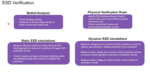
As analog and mixed-signal designs become increasingly complex, parasitic effects dominate both design time and cost, consuming 30–50% of engineers’ effort in debugging and reanalyzing circuits. Addressing these multiphysics effects requires early verification strategies and reliable simulation solutions. Modern … Read More
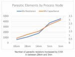
With advanced semiconductor processes continuing to shrink, the number and complexity of parasitic elements in designs grows exponentially contributing to one of the most significant bottlenecks in the design flow. Undetected parasitic-induced issues can be extremely costly, often resulting in tape-out delays.
Silvaco… Read More
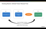
The development of electric vehicles (EVs) is key to transitioning to sustainable transportation. However, designing high-performance EVs presents significant challenges, particularly in power module design. Power modules, including inverters, bulky DC capacitors, power management ICs (PMICs), and battery packs, … Read More
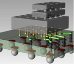
One of the most promising advancements in the semiconductor field is the development of 3D Integrated Circuits (3D ICs). 3D ICs enable companies to partition semiconductor designs and seamlessly integrate silicon Intellectual Property (IP) at the most suitable process nodes and processes. This strategic partitioning yields… Read More
In previous design generations interconnect could safely be modeled by extraction using just R and C values. Parasitics in interconnect are important because they can affect the operating frequency or phase error in circuits like VCO’s. The need to model parasitics properly in wires is just as applicable in PA’s, LNA’s and for… Read More