Introduction of 2.5D and 3D multi-die based products are helping extend the boundaries of Moore’s Law, overcoming limitations in speed and capacity for high-end computational tasks. In spite of its critical function within the 3DIC paradigm, the interposer die’s role and related challenges are often neither fully comprehended nor appreciated. A recent webinar hosted by Synopsys included presenters from AMD sharing their experiences in detail on a comprehensive design flow, which is based on Synopsys’ 3DIC Compiler platform, that addresses opportunities across floorplanning, construction, extraction, and signoff. The MI300X platform is designed to deliver exceptional performance for AI and HPC. It uses state-of-the-art die stacking and chiplet technology in a multi-die architecture that enables dense compute and high bandwidth memory integration.

Evolution of Packaging Technology
Packaging technology has significantly evolved to meet the increasing complexity of multi-die designs. Initially, organic substrates supported around 100 I/O connections per square millimeter, but modern techniques like hybrid bonding now enable over 100 million I/O connections per square millimeter. This evolution enhances integration and communication between dies, boosting overall system performance and enabling more compact and efficient designs essential for high-performance computing. The shift from organic substrates to advanced hybrid bonding marks a major advancement in supporting multi-die architectures, pushing the limits of speed, capacity, and integration.
Key technologies include:
C4 (Controlled Collapse Chip Connection): Used for pitches greater than 75 µm, suitable for applications with larger pitch sizes.
Microbumps: Provide finer pitches around 15 µm, enabling higher interconnect density for more integrated and compact designs.
Hybrid Cu (Copper) Bonding: Allows extremely tight pitches as small as 1 µm, offering high interconnect density and improved electrical and thermal performance.
These technologies facilitate the stacking of different chip types within a single package, supporting the development of powerful, efficient, and compact electronic systems.
The 3DIC Device Ecosystem
The 3DIC device ecosystem includes a variety of design styles and technologies such as CoWoS-S/R/L, InFO_oS, and SolC_H, each requiring different routing standards like HBM, and UCle. With such an array of technologies and design styles available for 3DIC integration, there come many challenges.
Challenges Faced
Floorplanning complexities arise from manual calculations and a lack of automation for bump mapping between dies, complicated by the risk introduced by alterations prior to 3D assembly. Construction faces a dilemma between slow manual custom layout and auto-routing tools ill-equipped for 3DIC-specific challenges, necessitating meticulous constraint management. Incorporating a 3D solver becomes imperative here for addressing complex routing issues effectively. Extraction struggles with standard RC methods to capture intricate package-style constructs and mitigate parasitic inductance on critical nets, necessitating the use of a Full Wave 3D solver for accurate RLC extraction, despite its labor-intensive nature. Finally, signoff encounters hurdles in static timing analysis (STA) due to the lack of inductance support, coupled with manual and non-scalable RLC extraction processes. This calls for integration of 3D solvers to model and analyze parasitic effects accurately within 3DIC architectures. These challenges underscore the critical need for innovative solutions to advance semiconductor design efficiency and reliability.
Advancing 3DIC Solutions
The focus should be on automation, smarter functionality, faster results, and reduced human intervention. Key strategies should include developing advanced algorithms for automating design tasks, integrating machine learning for intelligent suggestions, implementing parallel processing for speed, and optimizing workflows. Additionally, adopting constraint-aware design methodologies and automatic ECO generation will minimize manual intervention. Continuous improvement through feedback loops and agile development, along with enhanced verification and reliability-aware design techniques, will ensure high-quality and reliable products.
Synopsys 3DIC Compiler Platform
The Synopsys 3DIC Compiler platform and related tools address the challenges discussed above. The platform offers a simple command to mirror bumps between dies and automatically accounts for rotations, flips, optical shrinks and other complications. It enables die-to-die signal routing to support silicon-style 90-degree and 45-degree routing as well as PKG-style routing involving teardrops, degassing, etc. Matched-length, matched-pattern routing characterisitc of HBM subsystems are well supported with shielding to ensure signal integrity. Both RC and RLC extraction are supported from within the 3DIC Compiler platform, leaving it to the designer to choose between faster turnaround and best accuracy as appropriate and applicable.

Summary
The Synopsys 3DIC Compiler integrates various design stages and supports diverse technologies. Advanced automation and embedded AI technology enable intelligent routing and predictive analysis, reducing manual efforts. While there is always room for more automation features for 3DIC, the Synopsys 3DIC Compiler platform is a significant leap ahead of current generation solutions.
You can watch the webinar on-demand here.
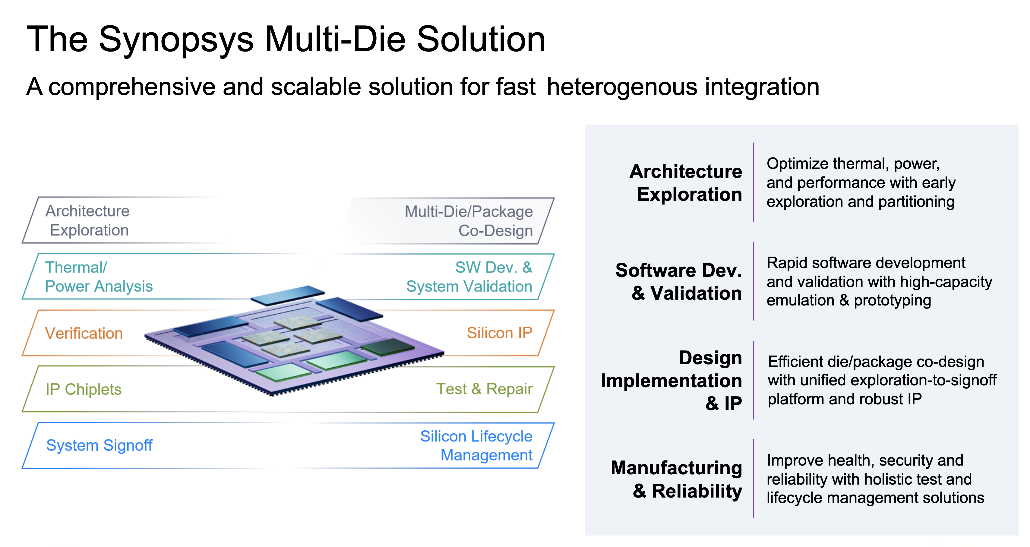
To learn more, visit the Synopsys Multi-Die Solution page.
Also Read:
Reduce Risk, Ensure Compliance: Hardware-Assisted Verification for Design Certification
What to Do with All that Data – AI-driven Analysis Can Help
Synopsys Accelerates Innovation on TSMC Advanced Processes
Share this post via:


Comments
There are no comments yet.
You must register or log in to view/post comments.