Everyone saw Shift Left, the EDA blockbuster. Digital logic design, with perfect 1s and 0s simulated through perfect switches, shifted into a higher gear. But the dark arts – RF systems, power supplies, and high-speed digital – didn’t shift smoothly. What do these practitioners need in EDA to see more benefits from shift left? Higher fidelity behavioral models. Authentic waveforms. Fast, accurate simulation schemes. And, looking forward, components with an “executable datasheet,” reproducing physical results when simulated in various contexts. Let’s go inside Keysight’s strategy in this series on how shift left gets a modulated signal makeover.
Unlocking more value across the ecosystem
The fundamental value of shift left – in fact, the whole purpose of EDA tools – is earlier visibility for design teams in virtual space. Waiting until problems show up in hardware drives up cost and risk and takes away flexibility. Earlier virtual validation reduces hardware re-spins with their trial-and-error. Teams can explore architectural options and avoid over-design trying to protect margins.
But shift left has the potential to unlock more value by pulling the ecosystem together. Project “visibility” improves when predictions show how close a design is to performance goals, and what remains to be done. Virtual sampling in the customer’s and the customer’s-customer contexts would help vendors demonstrate parts quickly and close sales faster.
Ultimately, shift left sets the stage for digital twins, enabling physical engineering activities to move to virtual space. For example, design teams and end customers would be able to gauge difficult physical experiences, like a satellite in orbit with interference, sun loading, jamming, and other dynamics. Digital twins need unprecedented levels of accuracy and trust in EDA tools.
Paving a two-way path for waveforms and data
When electromagnetic (EM) behaviors appear, these higher value wins only happen if modulated signals come to life in virtual space. Consider the case of a power amplifier (PA) designed using S-parameters and simulated with sine waves. Basic validation of a PA might fall apart when a team designs a hardware prototype around it and applies complex modulation like 5G or Wi-Fi 7.
Think about it this way: if testing with modulated signals is a given for hardware, why is it optional for simulating a design? The answer is most RF EDA workflows are one-way. They lack any path for bringing physical measurements back through simulation, either as a stimulus waveform or as improvements to behavioral modeling parameters. Bringing real-world effects back into a math-based model is at best applying a fudge factor with who knows what margin. When data and models don’t line up, system-level experiences get lost in translation.
Now consider Keysight’s vision for a two-way path with high-fidelity transportable models in a common modeling language. A device under test comes packaged with authentic waveforms and enhanced modeling data – an executable that goes beyond a datasheet. A single workflow connects design and simulation from detailed componentry to world-level scenario planning, enabling regression not possible with discontinuous point-based tools, waveforms, and data.
An example of why modulation is not an option
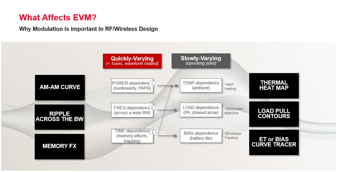
When shift left works for EM design, workflows must be two-way, and modulation is not an option. An example is error vector magnitude (EVM), a reliable figure of merit in wireless applications.
PA designers do an excellent job of focusing on power-dependent parameters, such as non-linearity and peak-to-average power ratio (PAPR). EVM outcomes rely on other important effects at work. Quickly varying effects determine performance in power, frequency, and time domains. Slower varying effects alter performance around temperature, load, and bias.

For example, a complex waveform can set off time-dependent memory effects that present as self-heating problems. Or wideband operation uncovers impedance mismatches at some points. Shouldn’t designers see those problems developing virtually, before getting surprised by measurements on a hardware prototype, or observations from a distant deployed platform?
Most EDA approaches have models that look at one affect at a time. Modern EM problems have more interrelated dimensions, and demand simulation of combinations of effects. Keysight provides a unique approach, blending EDA and test and measurement expertise, to see deeper. Modulated signals are the key to bringing the customer into the design environment. That requires stronger simulation engines, higher fidelity models, multiple effects in play, and one workflow from schematic capture through validation.
How does this work? Here’s a new Keysight video on modulated signals in EVM performance, using test and measurement insights and simulation techniques getting faster results on complex waveforms with combined effects.
Beyond the “choose your own compliance adventure”
A final point on changes in the complex EM systems business. Systems now have carefully defined waveforms from industry specifications. Choosing your own compliance adventure with some random stimulus won’t get the job done. Teams using shift left with modulated signals in a Keysight EDA environment can demonstrate with confidence that a virtual design hits requirements before hardware materializes.
It’s true not only for RF communications systems, but also for adjacent markets. Switched-mode power supply design must hit EMI compliance profiles in many markets. High-speed digital design is now dictated by specifications like PCIe Gen 5 and DDR5. Shift left brings those specifications and their waveforms into view much sooner in the design cycle.
System complexity shouldn’t be left to the reader to solve alone. Keysight has invested in creating EDA tools and workflows for RF system design with world-class measurement science built in. Over the next installments in this series, we’ll see more detailed examples in Keysight’s EDA solutions for shift left with modulated signals. Next up: digital pre-distortion design.
Also read:
WEBINARS: Board-Level EM Simulation Reduces Late Respin Drama
Share this post via:


Comments
There are no comments yet.
You must register or log in to view/post comments.