Integrated wafer-level fanout (WLFO) packaging technology is emerging as a foundation for multi-die solutions. Mobile product applications require focus on both aggressive chip-to-chip interface performance, as well as the final package volume. Traditional multi-chip packages using PCB laminate substrates do not readily provide the performance nor density targets. To address these requirements, WLFO packages need to support both side-by-side and stacked vertical Package-on-Package (PoP) topologies, to minimize interface electrical length. And, the reconstituted, molded wafer needs to support thinning process steps, to minimize total volume.
The conventional process flow for WLFO packaging involves precise placement of known-good die (KGD) face-down on an adhesive carrier, then encapsulating the array of die in an underfill plus molding compound. The adhesive carrier is removed, and the reconstituted wafer provides the new substrate for:
- the addition of interconnect redistribution layers (RDL) on top of the die
- (laser-drilled) vias and metal deposition through the molding for stacked connectivity
- backside grinding
- backside interconnect redistribution for PoP (optional)
- BGA bumps
- separation of the final, multi-die configuration
The disadvantages of this flow primarily pertain to the dedication of KGD prior to the WLFO packaging steps. The defect density of the conventional WLFO process increases the cost of yield loss, as the KGD are encapsulated. For example, there is a risk of yield loss die shiftdue to warpage issues, related to the fabrication of the reconstituted wafer molding and subsequent RDL patterning.
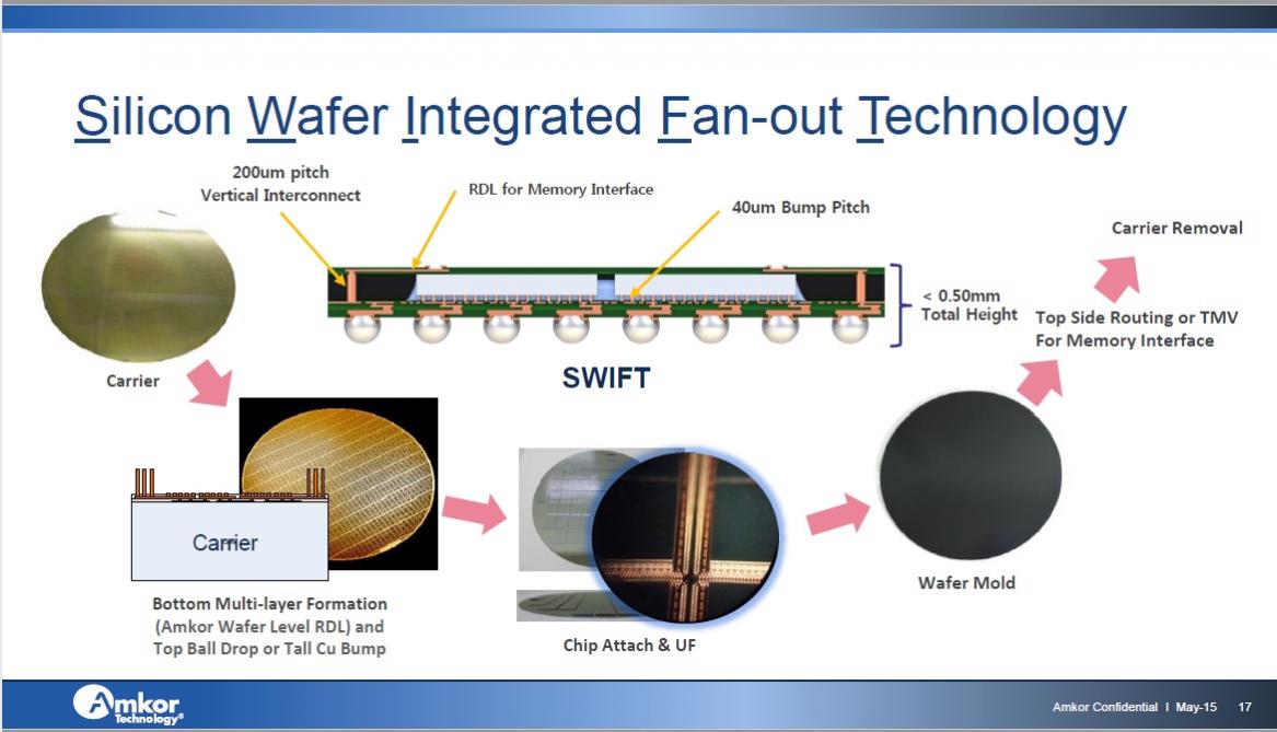
Amkor has developed an alternative process technology to address the yield/cost risks of the conventional WLFO flow. Rather than RDL patterning after molding, Amkor’s SWIFT (and SLIM) technology utilizes a pre-fabricated, known-good RDL structure that has been built on a separate carrier. The SWIFT assembly flow is illustrated in the figure below.

Figure 1. SWIFT assembly flow, highlighting the fabrication of a separate carrier for the RDL layers
The RDL build-up structure on the carrier is used for placement of KGD, with die microbumps for attach. After attach, underfill, and molding encapsulation, the carrier is removed an BGA bumps are attached.
The carrier flatness tolerance is tighter, compared to the conventional WLFO reconstituted wafer. As a result, Amkor’s SWIFT supports finer resolution RDL width/spacing patterning (which requires finer exposure depth-of-focus); and, the improved flatness allows additional RDL layers to be fabricated, a key benefit for today’s high I/O count SoC’s.
As a leading OSAT, Amkor’s interface with the foundry is flexible — either Amkor could fabricate the RDL structure on the carrier (SWIFT) or the foundry can do the processing (SLIM, with tighter RDL pitch fabrication available).
I recently had the opportunity to chat with Ron Huemoeller, VP Corporate R&D, Ruben Fuentes, VP Design Centers, and Curtis Zwenger, Senior Director Advanced Packaging and Technology Integration at Amkor, about their WLFO technology. John Park, Product Management Director at Cadence joined the discussion as well, to describe the latest for WLP support in Allegro, and to highlight results of the ongoing Cadence-Amkor collaboration.
John provided an insightful comment to level-set the discussion, “Advanced WLP is blurring the line between what is an IC and what is a package. Design enablement requires a mixture of IC and packaging design plus manufacturing rules for the fan-out RDL layers.”
Ron highlighted the complexity of the SWIFT and SLIM package designs, “We are supporting heterogeneous die integration, with each SoC potentially having thousands of I/O’s. The die attach and assembly to the SWIFT carrier needs to support a very fine I/O pitch — for example, copper pillars on a 30um pitch, 10 rows deep around the die.”
Ron continued, “An additional complexity factor is introduced by multi-chip packages which need to provide larger power and ground currents. We’ve added the capability to include an intermediate substrate in the packaging flow. This substrate includes both RDL connection layers, plus the option for thicker copper places for P/G distribution.”

Figure 2. SLIM-on-substrate package cross-section
The most intricate requirement for SWIFT technology is the PoP configuration. Ruben highlighted, “For a stacked PoP topology, the SWIFT carrier will include a pattern of tall copper pillars — Through Molding Vias (TMV). After molding and thinning to expose the pillars, additional redistribution wires can be added on the backside for subsequent PoP attach.”

Figure 3. Top RDL connected to TMV copper pillar, for package-on-package design
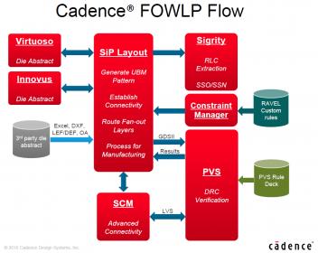
Given all these design complexities, and especially with the intricate design and manufacturability rules, Cadence and Amkor have released a “Package Assembly Design Kit” (PADK), to accelerate the productivity of SWIFT/SLIM package layout.
John provided additional background, “The widely-adopted Allegro Package Designer has been enhanced to support Advanced WLP Design (v.17.2). Package designers have access to productivity aids to assist with meeting package manufacturability requirements, such as the metal patterns needed for material outgassing and mechanical stress relief. The key feature is the integration of the Cadence Physical Verification System (PVS) to the APD environment. The sign-off flow uses IC fabrication runsets for DRC and LVS verification. The PADK is the Cadence/Amkor kit to enable this signoff-level verification.”

Figure 4. Cadence WLFO design and verification flowThere are unique data formatting requirements to enable running (batch) PVS from Allegro Package Designer. “Standard laminate package manufacturing uses the Gerber format. For WLP, mask making requires GDS-II streamed out from APD.”, John reminded me. “Package design geometries require accurate translation to IC process definitions. Circles, arcs, and trace ends require adaptation to GDS-II. Trace tapering and angled connections need special handling, as well.”
Executing LVS on the package connectivity requires exporting a Verilog (or CDL) netlist from APD, as well as the die placement data plus GDS-II for the RDL connections.
Error markers from PVS DRC and LVS are annotated back to the APD design platform to aid with debug.
What’s next for advanced wafer-level package design enablement? John indicated,“Given the interdependent nature of both IC and package technology design rules, Cadence is working to enable more interactive rule and constraint checking support. Our RAVEL rule definition tool can be used for in-design DRC for Allegro WLP design.”
Ron added, “We view this initial PADK release for SWIFT/SLIM as a first step in bridging the gap for WLP package design enablement. The physical verification runsets are just the first phase. This collaborative framework with Cadence will enable us to expand the scope of the WLP technology information for designers.”
Ron’s comment really rang true for me. The IC foundry industry fundamentally relies upon the PDK releases to customers, to enable design teams to develop their internal methodologies for implementation and tapeout signoff. The rapid advances in (multi-die) WLP technology require a similar level of technology and verification runset design enablement, to accelerate adoption. The PADK release announcement from Amkor and Cadence is an defining step in this strategic direction.
For more information on Amkor’s SWIFT/SLIM technologies, please follow this link.
For more information on Cadence’s Advanced WLP product support, please follow this link.
All SWIFT and SLIM images courtesy of Amkor Technology, Inc.
-chipguy
Share this post via:


Comments
There are no comments yet.
You must register or log in to view/post comments.