IC layouts go through extensive design rule checking to ensure correctness, before being accepted for fabrication at a foundry or IDM. There’s something called the antenna effect that happens during chip manufacturing where plasma-induced damage (PID) can lower the reliability of MOSFET devices. Layout designers run Design Rule Checks (DRC) to find areas that violate PID and then make edits to pass all checks.
A traditional antenna design rule will measure the metal (or via) layer to MOSFET gate layer, and if the area ratio is too large then the layout must be fixed by adding a protection diode.
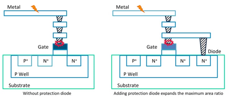
One IC layout scenario that a traditional DRC for antenna effects cannot handle is for AMS designs that have multiple power domains, using multiple isolated P-type wells as shown below. A new approach called path-based verification is required for the following four scenarios.
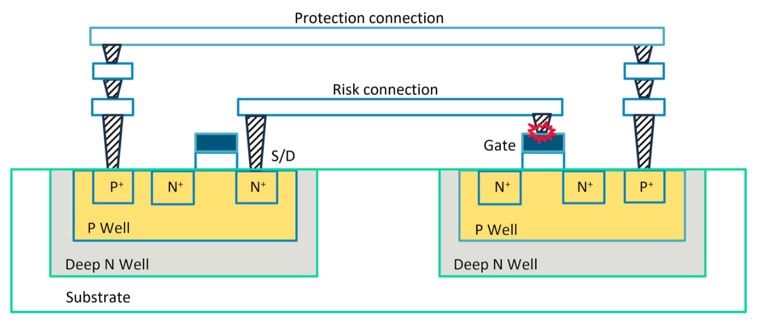
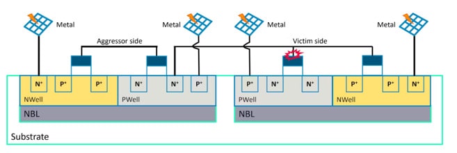
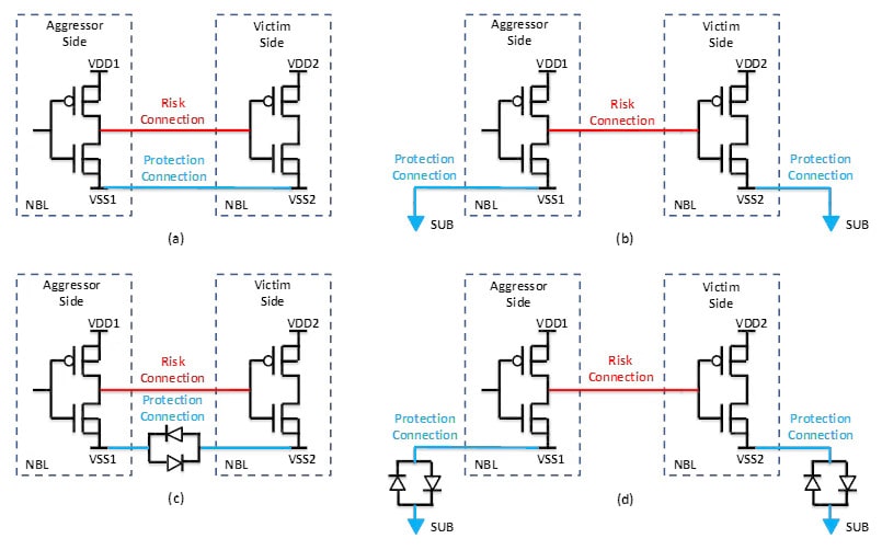
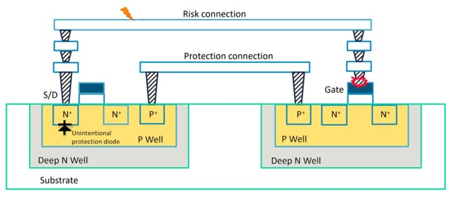
These four layout scenarios can only be detected by an EDA tool that knows about devices, connectivity and electrical paths during the area calculations for metal and MOSFET gate layers. This is where the Calibre PERC tool from Siemens EDA comes in, as it can perform the complex path-based checks to identify PID areas, find electrostatic discharge (ESD) issues, and locate other paths that your design group is looking for. Here’s the PID flow for using Caliber PERC:
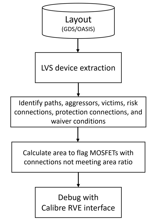
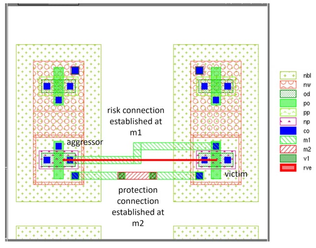
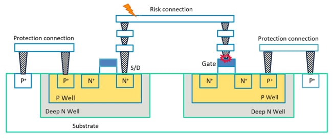
Using this flow on an IC layout and looking at the results in Calibre RVE results viewer showed that a PID violation was found, because a risk connection was established in metal1 level, but the protection connection didn’t happen until the metal2 level.
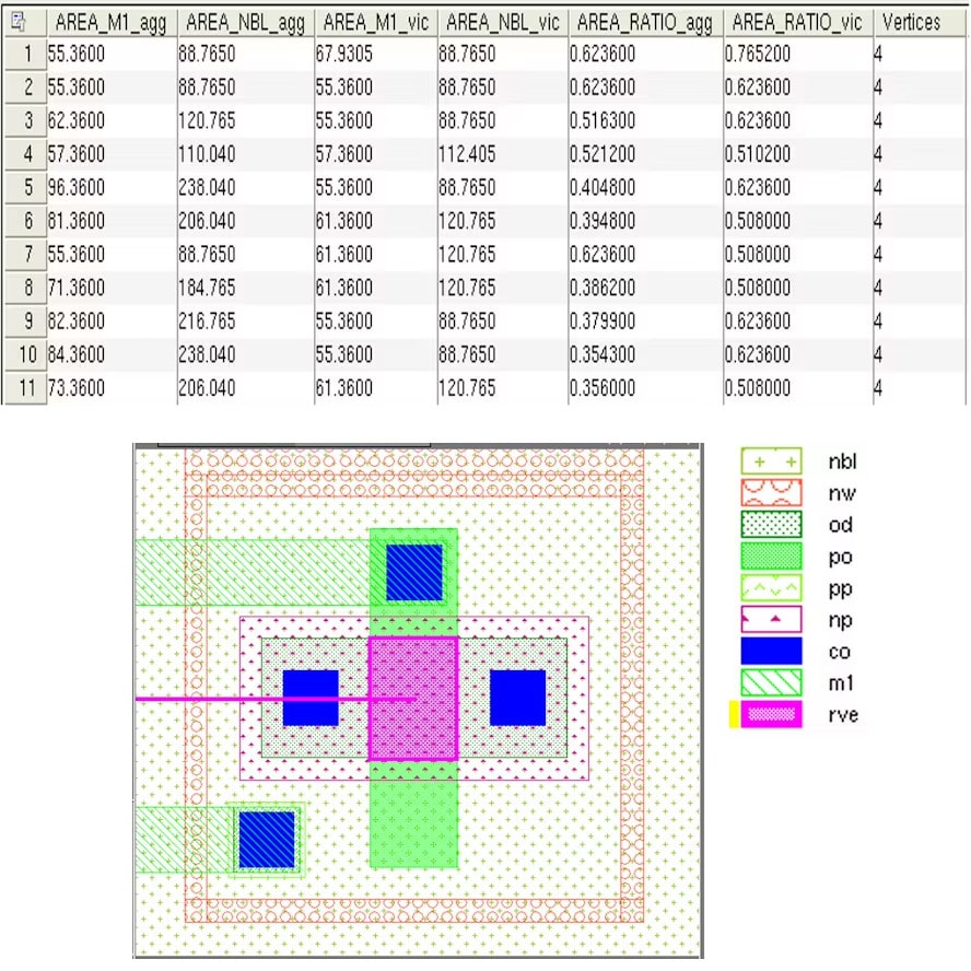
The next PID violation was identified from imbalanced area ratios of metal layer and the N-buried layer (nbl). The area highlighted in purple (rve) is the victim device.
To get complete PID coverage your design team will have to use both the traditional DRC-based antenna checks plus the path-based checks. Run DRC-type checks early in the design stages as a preventative step. As more metal connections in a layout are completed, then paths form across isolated P-type wells are made, it’s time to add path-based verification, providing complete coverage.
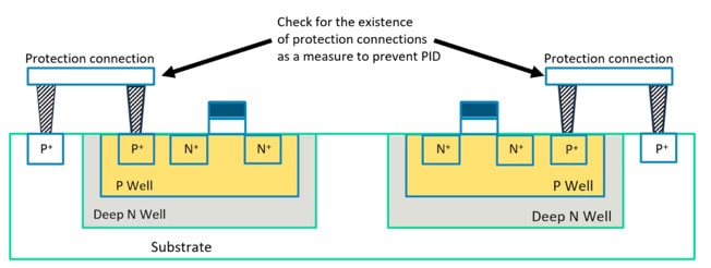
In this early IC layout it’s time to run traditional DRC-based antenna checks to confirm the layout passes PID validation.
As more metal paths are added to the IC layout, then it’s time to use the path-based tool, because it properly understands both the risk connection and protection connection.
Summary
IC layouts must meet rigorous design rules to pass reliability and yield requirements set by the foundry or fab process being used. Traditional DRC-based antenna design rules can still be used for early-stage layout, but as more metal layers are added to complete the interconnects, then a path-based checking with Calibre PERC becomes necessary.
As the paths across isolated P-wells are established, the path-based flow of Calibre PERC can be used to check the IC layouts at IP, block/module and even full-chip levels for signoff. So it’s recommended to use both flows together to meet the reliability and yield goals.
Read the Technical Paper at Siemens online.
Related Blogs
- Optimizing Shift-Left Physical Verification Flows with Calibre
- Calibre IC Manufacturing papers at SPIE 2023
- IC Layout Symmetry Challenges
- EDA in the Cloud with Siemens EDA at #59DAC
- Calibre, Google and AMD Talk about Surge Compute at #59DAC


Comments
2 Replies to “Checking and Fixing Antenna Effects in IC Layouts”
You must register or log in to view/post comments.