Understanding the electromagnetic (EM) coupling between various elements of a high-frequency semiconductor device is vital for meeting design specifications and ensuring reliable operation in the field. These EM interactions include not only the silicon chip but also extend to the package that encloses it. However, it may be only towards the end of a project that the IC or systems designer gets round to create and simulate EM models that include both on-die metals as well as the package layers. It is not uncommon to find that the inclusion of the package layers with the on-die metals model causes a degradation in performance that may cause specifications to be violated. To avoid this, Ansys provides a solution that can easily add package layers to a silicon technology’s metal stack-up in order to extract complete models with both on-silicon and package layers early in the design process.
Ansys’ suite of on-chip electromagnetic analysis tools operate on IC layouts at the pre-LVS design stage (Ansys RaptorX™) and the post-LVS signoff stage (Ansys Exalto™). The chip analysis can include portions of the package layout and/or package layers to extract a complete EM model that can be simulated with a SPICE circuit simulator. The Ansys tools rely on precise information about the interconnect process technology used in the manufacture of each layer. Process information is provided by silicon foundries in various formats, including Design Rule Manuals (DRMs) and technology files – such as iRCX, ITF, and ICT files – that may be unencrypted or encrypted. The process for capturing the technology stack-up compiles a collection of Ansys format technology files by mapping foundry provided process technology information onto physical layout information in OpenAccess or GDSII stream format (see Figure 1). These compiled technology files also support other Ansys on-chip EM tools including Ansys VeloceRF™ (inductive device layout synthesis) and Ansys RaptorQu™ (for superconducting quantum design).
RaptorX is a silicon-optimized electromagnetic solver, and it comes with a very useful wizard called Process Configurator that makes it easy to create and modify Ansys technology files, even for complex chip-package configurations. As shown in Figure 1, Process Configurator creates Ansys technology files that can contain just the foundry metal stack-up or can contain the foundry metal stack-up plus selected additional package layers. The input to the Process Configurator wizard for the foundry metal stack-up is the process information provided by the foundry. If die and package layers need to be co-extracted, then the package layer information for the layers of interest also needs to be included.
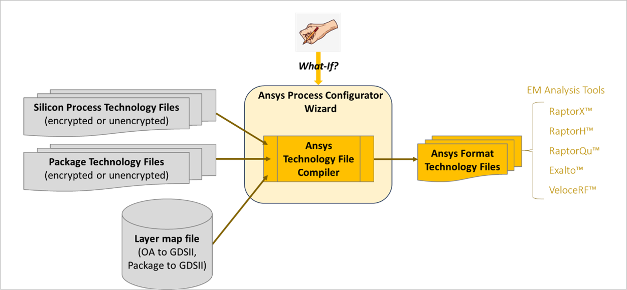
If the foundry technology file is unencrypted, or the package layer information is unencrypted, the Process Configurator wizard will let you explore various process-related “what-if” scenarios by editing the properties of the die and/or package layers and compiling different versions of the Ansys technology files. The Process Configurator allows designers to add or subtract substrates, backplanes, conductors, dielectrics, and vias including Through-Silicon Vias (TSV). The technology properties that can be edited with Process Configurator are metal thickness, metal conductivity, dielectric thickness, and dielectric constant. In order to complete the Ansys technology files the compiler also requires the GDS stream layer map file and the layer mapping information.
Some examples of modifying an unencrypted technology for “what-if” experiments include:
- modifying the substrate thickness and properties to explore effects of coupling through the substrate
- adding TSVs in an exploratory 3DIC stack up
- setting up a technology file for Wafer-on-Wafer (WoW) technology
adding package layers to see their effect on the EM device – as will be shown in the following example
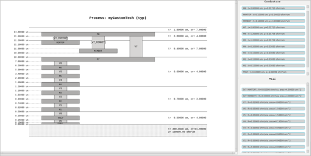
The input files and information for Process Configurator can be processed using both a UI and a batch-mode command script . The outputs of Process Configurator are the compiled Ansys process technology files used by the Ansys EM tool suite. The Process Configurator has the very useful capability to visualize a technology cross-section, which makes it easy to verify the correct sequence and connectivity of the technology layers. Unencrypted technology layer properties like thickness, resistivity, and dielectric constant are also displayed in the cross-section viewer. If the technology is encrypted then the cross-section viewer shows the layer sequence and connectivity, but the layer thicknesses are not to scale, and material properties are not reported.
Figure 2 below shows a stack up of a fictional example technology file. The left panel displays the substrate characteristics on the bottom layer, the cumulative layer height starting from the substrate, the layer and via names on the left, and the dielectric thickness and dielectric constant (er) on the right. The Conductor section in the right panel lists the conductors with their thickness and resistivity (r), and the Vias section shows the via resistance and area.
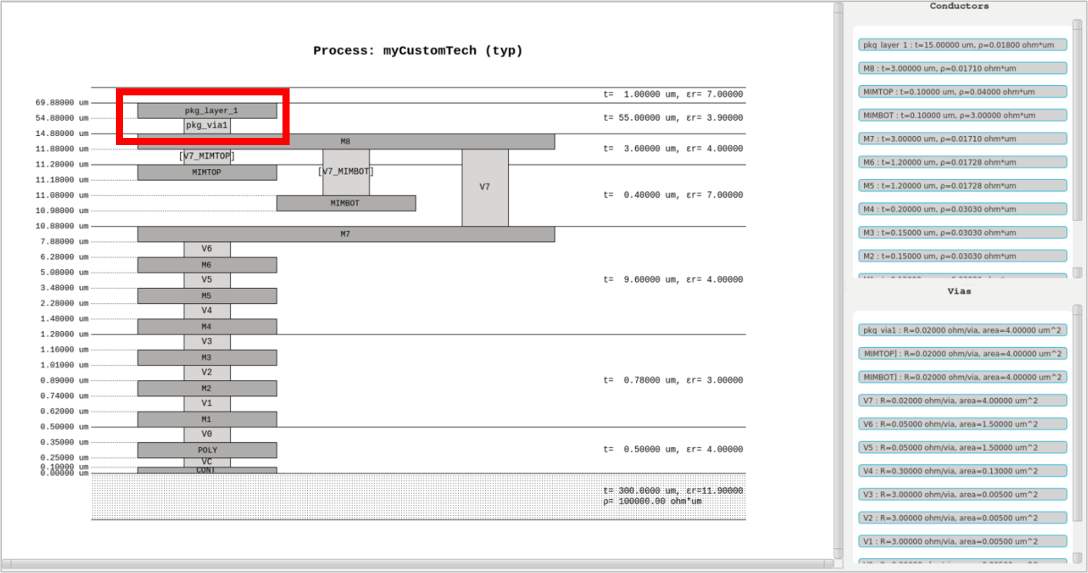
The red box in Figure 3 below highlights a via and package layer that have been added to the stack-up. This stack-up, with the package layer and via included, was used for the simulation results described in the following paragraphs that show how the package layer can affect the performance of an EM device.
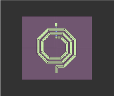
To illustrate how Process Configurator can be used to explore the effect of a package on a chip we created a simple layout example: It consists of an EM device – a single-ended octagonal spiral inductor – that was extracted using RaptorX. The resulting electrical model was then simulated in a SPICE-level circuit simulator to analyze the performance first with, and then again without, a package layer placed above it. Figure 4 below shows RaptorX’s physical mesh for the inductor without the package layer.

Next, the same inductor was used, but a rectangle of the package layer was placed above it. Figure 5 below shows the RaptorX mesh of the inductor with the package layer included.
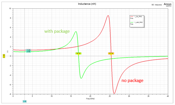
RaptorX generated an S-parameter model for each inductor, which were then simulated for Inductance and Quality Factor across a frequency range. Figure 6 shows the inductance of the two inductors plotted across frequency. Comparing the plot of inductance at 3 GHz for the package layer included (green) shows a 28% decrease in inductance, and 33% decrease in the resonance frequency versus the simulation results for the model without the package layer (red).
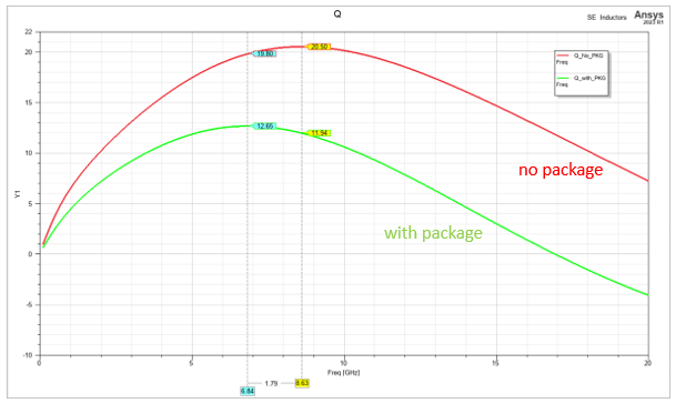
In Figure 7 below, the Quality Factor (Q) of the two inductors is plotted across frequency. Comparing the simulation plot of Q for the package layer included (green) shows a 38% decrease in Max Q value and a 21% decrease in max Q peak frequency versus the simulation results for the model without the package layer (red).
In summary, these simulation results illustrate the stark changes in device behavior that are seen when package layers are included in a simulation. Modeling package layers together with on-die metals can reveal degradation in performance that may violate a specification or cause the device to fail. Ansys has developed the Process Configurator to make it very easy for IC and System designers to capture even the most complex multi-layer packaging configurations and to facilitate quick experimentation. It encourages a shift-left approach with early what-if exploration to help designers find the best possible solution for optimizing their final product and avoid late-stage surprises.
Also Read:
Keynote Speakers Announced for IDEAS 2023 Digital Forum
Ansys Revving up for Automotive and 3D-IC Multiphysics Signoff at DAC 2023
Keynote Sneak Peek: Ansys CEO Ajei Gopal at Samsung SAFE Forum 2023
Share this post via:


Comments
There are no comments yet.
You must register or log in to view/post comments.