I just did a Google search for “3D IC”, and was stunned to see it return a whopping 476,000 results. This topic is trending, because more companies are using advanced IC packaging to meet their requirements, and yet the engineers doing the 3D IC design have new challenges to overcome. One of those challenges is creating a system-level netlist so that 3D netlist verification tools can be run to ensure that there are no connectivity errors.
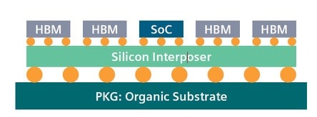
Here’s a cross-section of a 2.5D IC with chiplets containing multiple HBM and an SoC, using a silicon interposer with an organic substrate. Connectivity of this system could be captured in a Verilog netlist format, or even a CDL/SPICE format.

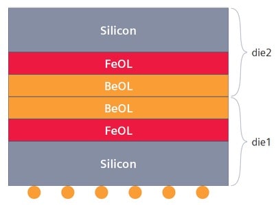
Stacking chips in 3D face-to-face is another advanced packaging method.

Chip engineers and package engineers often use different tools and flows to solve issues like connectivity. Ideally, there would be a system-level connectivity flow that understands both the chip and package domains.
Siemens EDA is a vendor that has tools that span both realms of IC and packaging, and their connectivity product is called Xpedition Substrate Integrator (xSI). With the xSI tool an engineer can import multiple die, interposer, package and PCB abstracts, then build a system-level model of the connectivity. After a system-level netlist has been exported from xSI, it’s ready to be used by an LVS tool like Calibre.
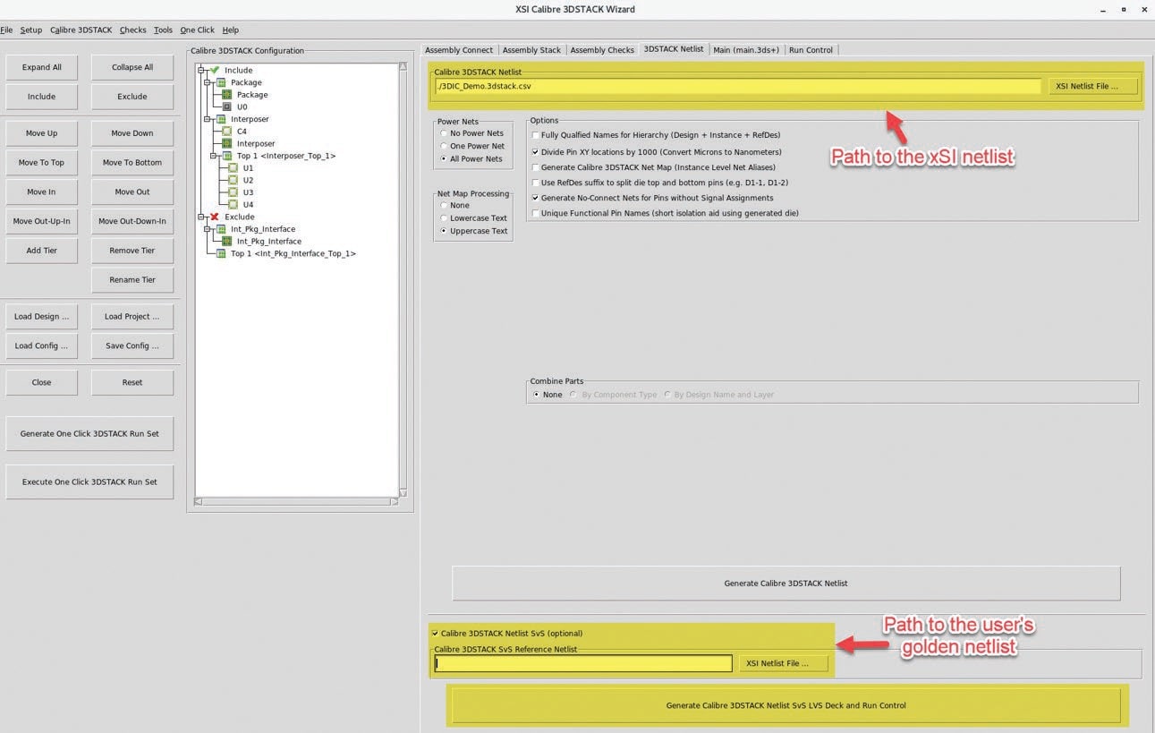
Running Calibre in netlist versus netlist mode is a method to check that the system-level netlist from xSI matches each chip netlist. The xSI tool has a wizard GUI to help you create a Calibre 3DSTACK netlist and run control.

The Calibre runset takes care of netlist conversions, die name mapping between IC and package, and any desired Calibre options. A clean report means that xSI was used properly to build a system connectivity.
For 3D-IC designs the silicon interposer could be in CDL or Verilog format, but the organic substrate is designed by the packaging group using CSV or ODB++ format. Designers may need to short or open certain signals, but that would result in LVS comparison errors.
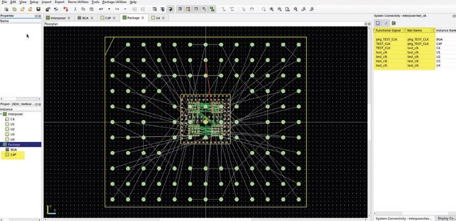
For a multi substrate 3D-IC design, using a silicon interposer plus organic substrate, the package team could user one name for a net, while the interposer team uses a different name for the same net. With xSI there’s a way to make this connection between two different net names, it’s called an interface part.
As an example, the following interposer has a net TEST_CLK, which is connected to the package substrate net pkg_TEST_CLK. The interface part allows these two differently name nets to be connected, and then running Calibre 3DSTACK will produce no false LVS errors.

Sometimes in a 3D-IC assembly you need to short unneeded signals to ground, or even short two power planes together, but these nets are not connected in the system netlist. While creating the source netlist for Calibre 3DSTACK you can create a shorts list with the net mapping feature.
Summary
3D netlists present challenges to the IC and package design process, so Siemens EDA has come up with a tool flow using xSI and Calibre tools. Building the correct system-level netlist is validated by running a netlist vs netlist comparison. When you need to account for opens and shorts, then they can be waived by design. Even different net names between package and interposer design teams are supported with this flow of xSI and Calibre.
The complete nine-page white paper is online here.
Related Blogs
- Five Key Workflows For 3D IC Packaging Success
- EDA in the Cloud with Siemens EDA at #59DAC
- 3D IC Update from User2User
- SIP Modules Solve Numerous Scaling Problems – But Introduce New Issues
- Mentor unpacks LVS and LVL issues around advanced packaging


Comments
There are no comments yet.
You must register or log in to view/post comments.