


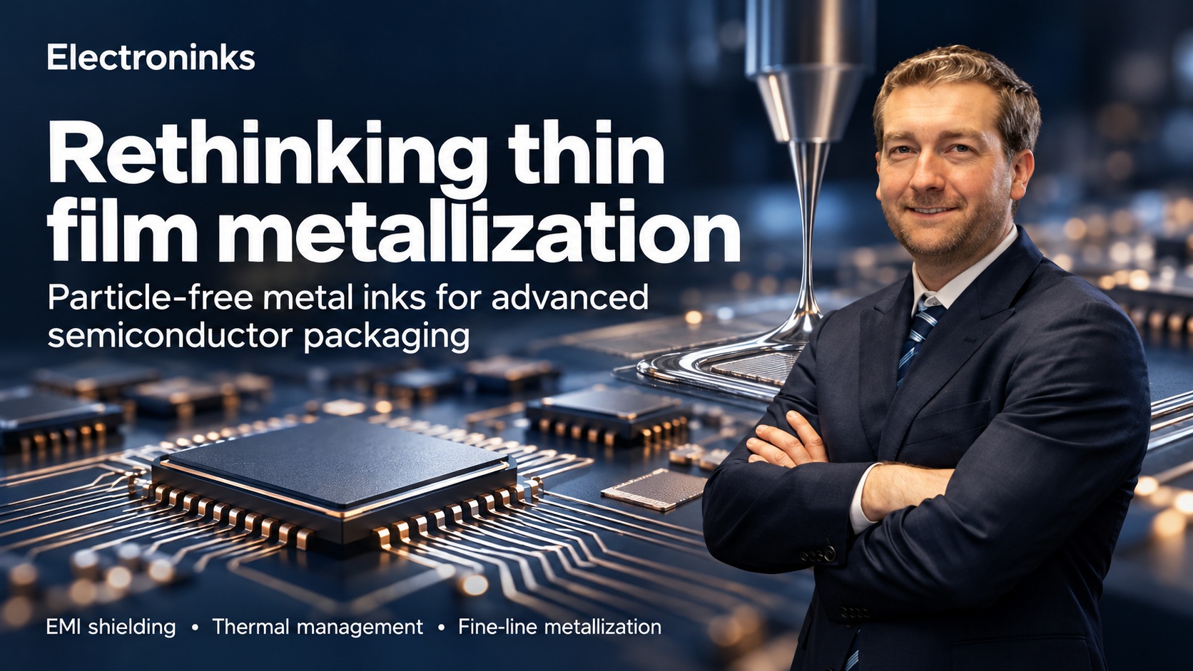



S. Brett Walker, Ph.D. is the Co-Founder and CEO of Electroninks and has extensive Materials Science experience. Dr. Walker built Electroninks, Inc. to over $1M in revenue after 1 year in business. He has also successfully introduced Circuit Scribe, a consumer electronic prototyping product via wildly successful kick starter campaign that raised $675, 425 in just a little over a month. His work on reactive silver inks named one of nine materials that will change the future of manufacturing by Scientific American. Dr. Walker was named as one of Forbes 30 under 30 for Manufacturing in 2015 and holds seven patents for novel ink formulations.
Tell us about your company.
Electroninks is an advanced materials company focused on thin film metallization, based in Austin, Texas. Our approach uses metal-organic decomposition, or MOD, chemistry. Our inks are particle-free metal complexes: they are applied as a liquid and cured at low temperature, leaving a polycrystalline metallic film.
That allows metal to be deposited using traditional patterning equipment in ambient environments, without complex vacuum equipment. Our portfolio spans silver, gold, platinum, nickel and copper inks, serving semiconductor packaging, printed circuit board manufacturing and defense applications, as well as consumer electronics, wearables and medical devices.
What problems are you solving?
Every advanced package needs metal in precise places, both to carry signals and to shield the chip. Today that metal is typically deposited by electroless plating or physical vapor deposition, which bring large equipment, significant floor space and demanding process chemistry.
Our materials are designed to deliver performance competitive with electroless or PVD metals, with high electrical conductivity, while plugging into existing deposition processes. Because the process is additive, metal goes only where it is needed.
The same logic applies to backside metallization for AI and high-performance computing chips, where heat dissipation is now a design constraint. Conventional sputtering and plating raise issues of cost, equipment, scaling to larger panels and environmental impact. Our approach aims to simplify that step.
What application areas are your strongest?
We see significant opportunities in back-end semiconductor packaging, where EMI shielding and thermal management are front and center.
In EMI shielding, our EI-1207 silver ink, part of the EI-1200 series, is sprayed onto packages and cures at 160 degrees Celsius. Our recon-free process coats package sidewalls well enough to remove the dicing and reconstitution steps that sputtered films normally require. We have reported shielding of 60 dB at 1.2 micrometers and 80 dB at 3 micrometers across 1 to 40 GHz. Silver can discolor under heat or humidity testing; that change is cosmetic and does not affect conductivity or shielding, and it can be addressed through chemistry changes or a black or clear overcoat.
In thermal management, we are working with Merck KGaA, Darmstadt, Germany on backside metallization. A spin-coated MOD layer bonds reliably with thermal interface materials and can replace multilayer metal stacks, and the technology is being commercialized at customer sites globally. The two companies plan to market it together, with on-site technical support in the United States and Asia Pacific.
We also see opportunities in seed layers for fine-line metallization and redistribution layers, where our copper MOD ink is intended to displace electroless copper plating and PVD tie layers. And we see opportunities in defense. Our earlier Phase II SBIR contract with the Air Force Rapid Sustainment Office, awarded in 2021, focused on printing PCBs on demand at the point of use. In July 2026 we were selected for an AFWERX Small Business Innovation Research contract to advance our CircuitJet platform for on-demand PCB manufacturing, and we have a memorandum of understanding with LIG Nex1 on lightweight, lower-cost antenna materials.
What keeps your customers up at night?
Ever increasing material specification requirements, and the infrastructure and footprint costs associated with electroless and vacuum-based metal deposition.
Packages are also getting more compact and complex. As system-in-package and heterogeneous integration spread, customers need shielding and metallization that can be applied selectively, without adding capital equipment or process steps.
What does the competitive landscape look like and how do you differentiate?
When most advanced thin film metals are deposited, electroless or physical vapor deposition is typically used. For EMI shielding, our spray process uses more than 99 percent less power and water than sputtering, and eight spray coaters fit in the floor space of one PVD system.
Sputtering is a line-of-sight process. Ours is not, which is why we can reach up to 100 percent sidewall coverage compared with about 40 percent for PVD. Third-party modeling by Savansys indicates up to 50 percent lower cost per package.
Our inks can be applied with existing spray, screen, inkjet and spin coating equipment, so they plug into infrastructure customers already have. Because the metal is deposited additively, material utilization is high: the silver ends up on the product, not lost in the process.
What new features and technology are you working on?
Electroninks has been making significant advances with its oxygen-tolerant copper MOD chemistry. We launched our copper MOD ink in September 2024 for seed layer printing, with grades for adhesion to glass, silicon and epoxy molding compound. At launch we showed a copper seed layer of about 100 nanometers, spin-coated on a wafer, and the ink can also be applied by spray, screen printing or inkjet.
In June 2026 we introduced an air-curable version. It cures in open air at about 150 degrees Celsius in 5 to 10 minutes, without inert gas, vacuum equipment or specialty tooling. Early results are on polyimide, glass, epoxy molding compound and build-up film, and we see it as a lower-cost alternative to silver and gold for large-area metallization. We are working with a select group of development partners.
We are also using AI-guided research, in work with Citrine Informatics, to improve our particle-free silver ink for aerosol jet printing, and we plan to apply the same approach to our gold and copper inks.
How do customers normally engage with your company?
Customers can engage with us directly, through our website, or through partners including Insulectro, SIIX in Japan, and Baba Fine Chemicals in India.
Our work with SIIX, for example, is starting with prototype trials of spray-coated EMI shielding on complex geometries such as automotive control units. Each engagement defines the coating approach with the customer rather than assuming a fixed recipe.
In India, Baba Fine Chemicals is our distribution partner, and together we are participating in the national IDSPS program. Many Indian packaging lines are greenfield builds, which gives customers a rare opportunity to design next-generation shielding and metallization processes in from the start.


The $725 Million Chip Development: Why Execution Risk, Not IP Cost, Now Dictates Advanced-Node Survival