You are currently viewing SemiWiki as a guest which gives you limited access to the site. To view blog comments and experience other SemiWiki features you must be a registered member. Registration is fast, simple, and absolutely free so please,
join our community today!
            WP_Term Object
(
    [term_id] => 24
    [name] => TSMC
    [slug] => tsmc
    [term_group] => 0
    [term_taxonomy_id] => 24
    [taxonomy] => category
    [description] =>
    [parent] => 158
    [count] => 621
    [filter] => raw
    [cat_ID] => 24
    [category_count] => 621
    [category_description] =>
    [cat_name] => TSMC
    [category_nicename] => tsmc
    [category_parent] => 158
    [is_post] =>
)

WP_Term Object
(
    [term_id] => 24
    [name] => TSMC
    [slug] => tsmc
    [term_group] => 0
    [term_taxonomy_id] => 24
    [taxonomy] => category
    [description] =>
    [parent] => 158
    [count] => 621
    [filter] => raw
    [cat_ID] => 24
    [category_count] => 621
    [category_description] =>
    [cat_name] => TSMC
    [category_nicename] => tsmc
    [category_parent] => 158
    [is_post] =>
)
TSMC originally brought the pure-play foundry business to the United States in 1996 through a joint venture with customers Altera, Analog Devices, ISSI, and private investors (no government money). Altera is now part of Intel but ADI is still a top TSMC customer and enthusiastic supporter. I have seen the ADI CEO Vincent Roche … Read More
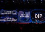
This is the 15th anniversary of the TSMC Open Innovation Platform (OIP). The OIP Ecosystem Forum will kick off on September 27th in Santa Clara, California and continue around the world for the next two months in person and on-line in North America, Europe, China, Japan, Taiwan, and Israel. These are THE most attended semiconductor… Read More
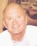
During my research I found an interview with Don Brooks from February 2000. It was very interesting and confirmed some of the things I knew about Don and brought up a few things I did not know. It’s an hour but it is a video of Don telling his story and is definitely worth a look. One of the things that was not mentioned however is the… Read More
Don Brooks is well known to many long time semiconductor insiders, like myself, but most SemiWiki readers have probably never heard of him. Don is a semiconductor legend and here is his story. This will be in two parts since he had a big impact on the semiconductor industry and TSMC. From 1991 to 1997 Don served as President of TSMC and… Read More
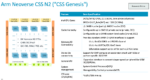
Arm just revealed at HotChips their compute subsystems (CSS) direction led by CSS N2. The intent behind CSS is to provide pre-integrated, optimized and validated subsystems to accelerate time to market for infrastructure system builders. Think HPC servers, wireless infrastructure, big edge systems for industry, city, enterprise… Read More
Most people ( including ChatGPT) think Morris Chang was the first TSMC CEO but it was in fact Jim Dykes, a very interesting character in the semiconductor industry.
According to his eulogy: Jim came from the humblest of beginnings, easily sharing that he grew up in a house without running water and never had a bed of his own. But because… Read More
Given the changes in the music business, the term “Rock Star” doesn’t really have any relevance to music or its performers anymore. Instead, we use the term to describe leaders, innovators and generally people or organizations of great significance. In the world of semiconductors, the designers of advanced chips were the rock… Read More
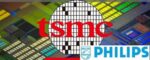
TSMC and Philips have deep historical ties. In fact, TSMC may not have existed without Philips. In the 1980s TSMC was established as a joint venture with Philips Electronics, the government of Taiwan, and other private investors. Several semiconductor companies were approached by Morris Chang for funding including semiconductor… Read More
High volume manufacturing is a 24/7 business with 12 hour shifts. You don’t always get to pick the shifts you want and you must cover for others when they can’t. It’s a challenging career and not for the faint of heart like myself.
In the 1980s and 1990s I spent time in Japan working with some of the top Japanese semiconductor manufacturers.… Read More
Now that semiconductors are front page news and a political football, I would like to write more about how we got to where we are today to better understand where semiconductors will go tomorrow. I will start this article with a provocative quote that really made me laugh and will put some context to what I am trying to accomplish here:… Read More