First, the TSMC Museum of Innovation is now open and it’s quite impressive. Located right below Fab 12, it is definitely worth an hour of your time. Second, Morris Chang was on the investor call which made it much more interesting, especially his comments on the recent Report to the President on U.S. semiconductor leadership. Third,… Read More

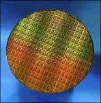
Making the Move from 28nm to FinFET!
If you click FinFET in the SemiWiki.com Latest News: navigation bar at the top of this page you will get a list of 86 blogs that have been viewed more than 600,000 times. If you go to the last blogs on the list, meaning the first blogs to be published, you will see a three part series, “Introduction to FinFET Technology” written by Tom Dillinger… Read More
Analog Bits and TSMC!
As a long time semiconductor IP professional I can tell you for a fact that it is one of the most challenging segments of semiconductor design. Given the growing criticality of semiconductor IP, the challenges of being a leading edge IP provider are increasing and may be at a breaking point. The question now is: What does it take to … Read More
2017 Semiconductor Dead Pool
In 2015 we saw $85B in semiconductor acquisition activity and in 2016 there was more than $110B. Given 2015 and 2016 were relatively flat years for the $335B semiconductor industry and 2017 looks like more of the same we should expect consolidation to continue, absolutely.
So, let’s come up with a list of companies that may fall in… Read More
The 2017 Leading Edge Semiconductor Landscape
In early September of 2016 I published an article “The 2016 Leading Edge Semiconductor Landscape” that proved to be very popular with many views, comments and reposting’s. Since I wrote that article a lot of new data has become available enabling some projections to be replaced by actual values and new analysis… Read More
Intel Spreadtrum ARM SoCs
In June of 2013 Edward Snowden copied and leaked classified information from the National Security Agency (NSA). His actions exposed numerous surveillance programs that many governments around the world reacted to, including China. In September of 2013 China Vice Premier Ma Kai declared semiconductors a key sector for the … Read More
IEDM 2016 – 7nm Shootout
In the first session of IEDM on Monday, December 5th there were two papers presented on 7nm processes. The first paper was from TSMC and the second paper was from the Global Alliance of GLOBALFOUNDRIES, IBM and Samsung.… Read More
IEDM 2016 – GLOBALFOUNDRIES 22FDX Update
At IEDM in 2015 I had a chance to sit down with Subramani (Subi) Kengeri and get a briefing on GLOBALFOUNDRIES 22FDX technology. At IEDM 2016 Rick Carter of GLOBALFOUNDRIES presented a paper on 22FDX. Following Rick’s presentation, I had a chance to sit down with Rick and John Pellerin, VP of Technology and Integration and … Read More
GLOBALFOUNDRIES ASIC Update!
Back in my IP days we spent a lot of time with the ASIC companies chasing multi-million dollar licensing deals. IBM was a fierce ASIC competitor back then with leading edge processes and a silicon proven IP catalog that was unmatched.
Unfortunately that ended at 65nm as the pure-play foundries (TSMC and UMC) and fabless ASIC companies… Read More
An End of Year View of Semi Consolidation
The last couple of years have been tumultuous for the semiconductor market. IC Insights just released a report showing just how much consolidation has concentrated market strength in a small number of companies. The report (which excludes fabs) shows that the 5 top companies – Intel, Samsung, Qualcomm, Broadcom and SK Hynix – … Read More
Musk’s Orbital Compute Vision: TERAFAB and the End of the Terrestrial Data Center