You are currently viewing SemiWiki as a guest which gives you limited access to the site. To view blog comments and experience other SemiWiki features you must be a registered member. Registration is fast, simple, and absolutely free so please,
join our community today!
WP_Term Object
(
    [term_id] => 158
    [name] => Semiconductor
    [slug] => semiconductor-manufacturers
    [term_group] => 0
    [term_taxonomy_id] => 158
    [taxonomy] => category
    [description] =>
    [parent] => 0
    [count] => 1406
    [filter] => raw
    [cat_ID] => 158
    [category_count] => 1406
    [category_description] =>
    [cat_name] => Semiconductor
    [category_nicename] => semiconductor-manufacturers
    [category_parent] => 0
    [is_post] =>
)
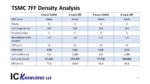
I have written a lot of articles looking at leading edge processes and comparing the process density. One comment I often get are that the process density numbers I present do not correlate with the actual transistor density on released products. A lot of people want to draw conclusions an Intel’s processes versus TSMC’s processes… Read More
The current Coronavirus crisis is inflicting a lot of pain on people, companies, and governments. I hope I am not getting in trouble with my reasoning, but if you look closely, there are also some “positives” to the Covid-19 crisis.
– It is stress-testing our infrastructure and telling us where we need to improve – as country,… Read More
On May 15th TSMC “announced its intention to build and operate an advanced semiconductor fab in the United States with the mutual understanding and commitment to support from the U.S. federal government and the State of Arizona.”
The fab will run TSMC’s 5nm technology and have a capacity of 20,000 wafers per month (wpm). Construction… Read More
-Could GloFo come back?
-TSMC or Intel or both or neither?
-Samsung would be a long shot?
-Perhaps Apple could convince TSMC?
The Wall Street Journal put out an article that detailed what we had indicated in our newsletter 10 days ago, that the US government is looking at getting a US based foundry to protect our interests given our … Read More
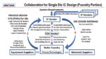
TSMC as Pure Play Wafer Foundry
TSMC started its wafer foundry business more than 30 years ago. Visionary management and creative engineering teams developed leading-edge process technologies and their reputation as trusted source for high-volume production. TSMC also recognized very early the importance of building an … Read More
Recently Seeking Alpha published an article “Taiwan Semiconductor Manufacturing Company Losing Its Process Leadership To Intel” and Dan Nenni (SemiWiki founder) asked me to take a look at the article and do my own analysis. This is a subject I have followed and published on for many years.
Before I dig into specific process density… Read More
We live in an age of abundant information. There is a tremendous exchange of ideas crisscrossing the world enabling new innovative type of products to pop up daily. Therefore, in this era there is a greater need to understand competitive intelligence. Corporate companies today are interested in what other competitors are brewing… Read More
Covid issues create “lumpy” quarters due to delays
Orders & demand remain solid and strong
2020 Year financials intact so far but ignore Qtrs
Taking prudent actions- no buybacks or guidance
As expected, Covid impacts both shipments & supply chain, ignore the near term lumpiness…
ASML reported revenues… Read More
TSMC has had an incredible run since its founding in 1987 which spans most of my 36 year semiconductor career. Even in these troubled times TSMC is a shining bellwether with double digit growth expectations while the semiconductor industry will be flat or slightly down. Let’s take a close look at the TSMC Q1 2020 conference call and… Read More
COVID-19 underscores the importance of US-based production for strategic industries
The COVID-19 pandemic has drawn intense focus on the need to repatriate pharmaceutical manufacturing back to the United States. The increased awareness that a strategic adversary manufactures or controls up to 80% of the active pharmaceutical… Read More


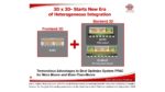

Enhancing Multi-Domain System Simulation with FMI Co-Simulation