You are currently viewing SemiWiki as a guest which gives you limited access to the site. To view blog comments and experience other SemiWiki features you must be a registered member. Registration is fast, simple, and absolutely free so please,
join our community today!
WP_Term Object
(
    [term_id] => 20
    [name] => Samsung Foundry
    [slug] => samsung-foundry
    [term_group] => 0
    [term_taxonomy_id] => 20
    [taxonomy] => category
    [description] =>
    [parent] => 158
    [count] => 135
    [filter] => raw
    [cat_ID] => 20
    [category_count] => 135
    [category_description] =>
    [cat_name] => Samsung Foundry
    [category_nicename] => samsung-foundry
    [category_parent] => 158
    [is_post] =>
)
In the history of the fabless semiconductor industry the foundries have always been a process node or two behind the leading semiconductor manufacturers. Starting in Q1 2017, for the first time in fabless semiconductor history, the foundries will have a process node advantage. This is horrible news for some but great news for … Read More
As the mobile industry growth slows and looks to growth in IoT, companies like Samsung Electronics are looking for ways to initiate change or adapt to the new climate around them. One of the ways mobile companies are going to be profitable in the future is through offering, building and sometimes hosting those services beyond just… Read More
An increasing percentage of SoC die area is being allocated to memory arrays, as applications require more data/instruction storage and boot firmware. Indeed, foundries invest considerable R&D resources into optimizing their array technology IP offerings, often with more aggressive device features than used for other… Read More
Most of the presentations from the FD-SOI Symposium in San Jose last month (April 2016) are now available on the SOI Consortium website (click here to see the full list — if they’re posted, you can download them freely from there). If you don’t have time to wade through them all, here are some of the highlights. … Read More
It is truly amazing to consider the advances in microelectronic process development, using 193i photolithography. The figure below is a stark reminder of the difference between the illuminating wavelength and the final imaged geometries. This technology evolution has been enabled by continued investment in mask data generation… Read More
For success, VR playback and content must be robust
The world of VR is split into two different areas, tethered PC VR and mobile VR. The reason why so many companies are going after mobile VR is because that’s where all of the volume is expected to be in VR. As a result, you have companies like Samsung Electronics and LG Electronics introducing… Read More
The latest generations of power efficient and full-featured applications processors in NXP’s very successful and broadly deployed i.MX platform are being manufactured on 28nm FD-SOI. The new i.MX 7 series leverages the 32-bit ARM v7-A core, targeting the general embedded, e-reader, medical, wearable and IoT markets, where… Read More
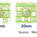
For more than a decade 2D NAND has been the leading driver of lithography shrinks, for example, Samsung went from 120nm in 2003 to 16nm in 2014 with shrinks on an almost yearly basis, but the shrinks came at a price. At 16nm Self Aligned Quadruple Pattering (SAQP) was required for the most critical layers and patterning related costs… Read More
Samsung Foundry had an intimate gathering recently for 200 customers and partners that I missed, but I know several people who attended. This event was a precursor to #53DAC where Samsung has the largest foundry presence. I was able to clarify what I had heard via a phone call with Kelvin Low so here is my version of what is important:… Read More
When I first heard about a foundry possibly licensing FD-SOI I would have bet it was SMIC in China. What better market for a low cost, low power, easy to manufacture alternative to FinFETs? The foundry of course was Samsung which also made complete sense since they have 28nm gate-first capacity that matches up nicely to 28nm FD-SOI.… Read More

Solving the EDA tool fragmentation crisis