You are currently viewing SemiWiki as a guest which gives you limited access to the site. To view blog comments and experience other SemiWiki features you must be a registered member. Registration is fast, simple, and absolutely free so please,
join our community today!
WP_Term Object
(
    [term_id] => 89
    [name] => FinFET
    [slug] => finfet
    [term_group] => 0
    [term_taxonomy_id] => 89
    [taxonomy] => category
    [description] =>
    [parent] => 0
    [count] => 231
    [filter] => raw
    [cat_ID] => 89
    [category_count] => 231
    [category_description] =>
    [cat_name] => FinFET
    [category_nicename] => finfet
    [category_parent] => 0
    [is_post] =>
)
On Thursday April 5th the Design and Reuse SoC IP days continues in Santa Clara at the Hyatt Regency (my favorite hangout). SemiWiki is a co-sponsor and I am Chairman of the IP Security Track. More than 400 people have registered thus far and I expect a big turnout, if you look at the program you will see why. You should also know that registration… Read More
Designers spend a lot of time looking at their layouts in 2D. This is done naturally because viewing in 2D is faster and simpler than in 3D. It helps that humans are good at extrapolating from 2D to 3D. Analysis software, such as extraction software also spend a lot of time looking at layouts in 2D. While this is fine for approximate results,… Read More
Design process retargeting is acommon recurrence based on scaling orBOM(Bill-Of-Material) cost improvement needs. This occursnot only with the availability of foundry process refresh to a more advanced node,but also to any new derivative process node tailored towards matching design complexity, power profile or reliability… Read More
We (SemiWiki) have been working with Fractal for close to five years now publishing 25 blogs that have garnered more than 100,000 views. Generally speaking QA people are seen as the unsung heroes of EDA since the only time you really hear about them is when something goes wrong and a tapeout is delayed or a chip is respun.
FinFETs really… Read More
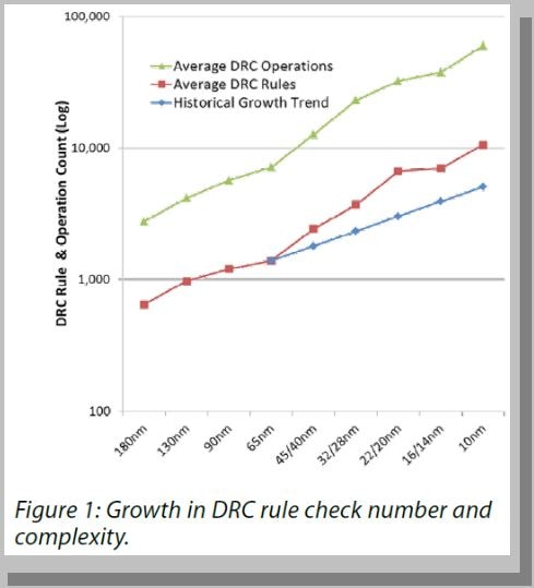
Variation analysis continues to be increasingly important as process technology moves to more advanced nodes. It comes as no surprise that tool development in this area has been vigorous and aggressive. New higher reliability IC applications, larger memory sizes and much higher production volumes require sophisticated yield… Read More
There’s been a lot of discussion of late about deep learning technology and its impact on many markets and products. A lot of the technology under discussion is basically hardware implementations of neural networks, a concept that’s been around for a while.
What’s new is the compute power that advanced semiconductor technology… Read More
At Intel back in the late 1970’s we wanted to know what process corner each DRAM chip and wafer was trending at so we included a handful of test transistors in the scribe lines between the active die. Having test transistors meant that we could do a quick electrical test at wafer probe time to measure the P and N channel transistor… Read More
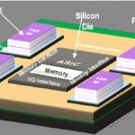
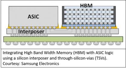
High Bandwidth Memory (HBM) systems have been successfully used for some time now in the network switching and high-performance computing (HPC) spaces. Now, adding fuel to the HBM fire, there is another market that shares similar system requirements as HPC and that is Artificial Intelligence (AI), especially AI systems doing… Read More
If you are interested in what types of chips we will see in the coming years always ask an ASIC provider because they know. Companies of all sizes (small-medium-large) use ASIC companies to get their chips out in the least amount of time and at a minimum cost because that is what ASIC companies do.
IP is an important ingredient to the … Read More
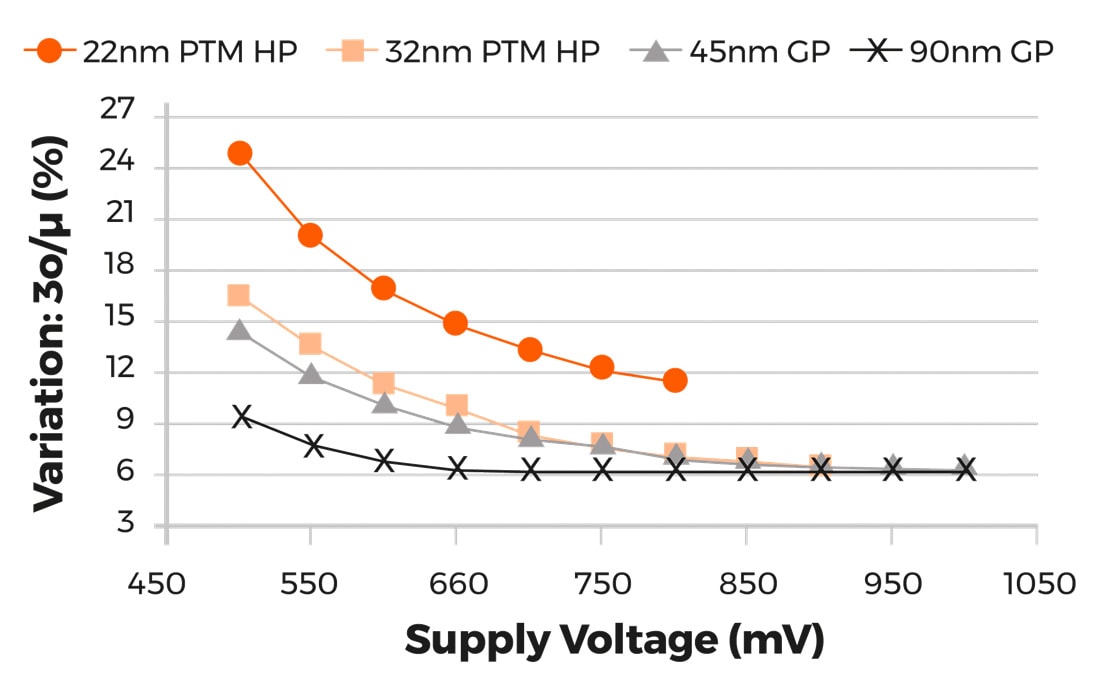
As I have said many times, IEDM is one of the premier conferences for semiconductor technology. On Sunday before the formal conference started I took the “Boosting Performance, Ensuring Reliability, Managing Variation in sub-5nm CMOS” short course. The second module in the course was “Multi-Vt Engineering… Read More


Musk’s Orbital Compute Vision: TERAFAB and the End of the Terrestrial Data Center