You are currently viewing SemiWiki as a guest which gives you limited access to the site. To view blog comments and experience other SemiWiki features you must be a registered member. Registration is fast, simple, and absolutely free so please,
join our community today!
WP_Term Object
(
    [term_id] => 50
    [name] => Events
    [slug] => events
    [term_group] => 0
    [term_taxonomy_id] => 50
    [taxonomy] => category
    [description] =>
    [parent] => 0
    [count] => 1556
    [filter] => raw
    [cat_ID] => 50
    [category_count] => 1556
    [category_description] =>
    [cat_name] => Events
    [category_nicename] => events
    [category_parent] => 0
    [is_post] =>
)
A huge theme at #54DAC this year was all things automotive and in particular the phrase ADAS (Assisted Driver Assistance Systems), so I followed up with Raja Tabet a corporate VP of emerging technology at Cadence. We met on Monday in a press room where I quickly learned that Cadence has been serving the automotive industry for the … Read More
I wrote up a quick article in the weeks before the Design Automation Conference (DAC) letting readers know that Integrated Photonics were indeed coming to DAC again this year. As a follow up, I attended the DAC presentation, ‘Capture the Light. An Integrated Photonics Design Solution from Cadence, Lumerical and PhoeniX Software’,… Read More
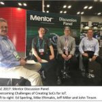
As the Internet of Things (IoT) opportunities continues to expand, companies are working hard to bring System-on-Chip (SoC) solutions to market in the hopes of garnering market share and revenue. However, it’s not as easy as it may first seem. Companies are running into a series of issues that stand between them and capturing the… Read More
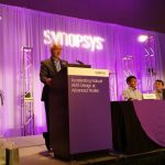
Every SoC that connects to an analog sensor or device requires AMS (Analog Mixed-Signal) circuit simulation for design and verification, so this year at #54DAC the organizers at Synopsys hosted another informative AMS panel session over lunch time on Monday. What makes this kind of panel so refreshing is that the invited speakers… Read More
At this year’s Design Automation Conference (DAC), TSMC unveiled more details about the design enablement platforms that were introduced at their 23[SUP]rd[/SUP] annual TSMC Technology Symposium earlier this year. I attended a presentation on TSMC’s Automotive Enablement Platform held at the Cadence Theater where TSMC’s… Read More
Last week at #54DAC there was a talk by Michael Yu from the CAD group of Oracle who discussed how they designed their latest generation of SPARC chips, with an emphasis on the reliability simulations. The three features of the latest SPARC family of chips are:
- Security in silicon
- SQL in silicon
- World’s fastest microprocessor
…
Read More
Right before #54DAC I participated in a webinar with Methodics on “New Concepts in Semiconductor IP Lifecycle Management” with Simon Butler, CEO of Methodics, Michael Munsey, Vice President of Business Development and Strategic Accounts, and Vishal Moondhra, Vice President of Applications. Thewebinar introduced… Read More
The Siemens purchase of Mentor last year for a premium $4.5B was a bit of a shock to me as I have stated before. I had an inkling a Mentor acquisition was coming but Siemens was not on my list of suitors. The reviews have been mixed and the Siemens commitment to the IC EDA market has been questioned so I spent some time on this at #54DAC.
First… Read More
This was my 34[SUP]th[/SUP] DAC, yes 34. It is a shame blogging did not exist back then because I would have liked to have read thoughts from my eager young mind, or maybe not. The first thing that struck me this year is the great content. Before DAC I review the sessions I want to see and this year there were many more than I had time for. … Read More
TSMC has been an ardent supporter of DAC for the last 18 years which has brought in the other foundries because, as the industry leader, wherever TSMC goes the other foundries naturally follow. The exception of course is Intel Custom Foundry because they march to the beat of a different drummer, if you know what I mean. The CoFluent… Read More

Enhancing Multi-Domain System Simulation with FMI Co-Simulation