You are currently viewing SemiWiki as a guest which gives you limited access to the site. To view blog comments and experience other SemiWiki features you must be a registered member. Registration is fast, simple, and absolutely free so please,
join our community today!
WP_Term Object
(
    [term_id] => 50
    [name] => Events
    [slug] => events
    [term_group] => 0
    [term_taxonomy_id] => 50
    [taxonomy] => category
    [description] =>
    [parent] => 0
    [count] => 1516
    [filter] => raw
    [cat_ID] => 50
    [category_count] => 1516
    [category_description] =>
    [cat_name] => Events
    [category_nicename] => events
    [category_parent] => 0
    [is_post] =>
)
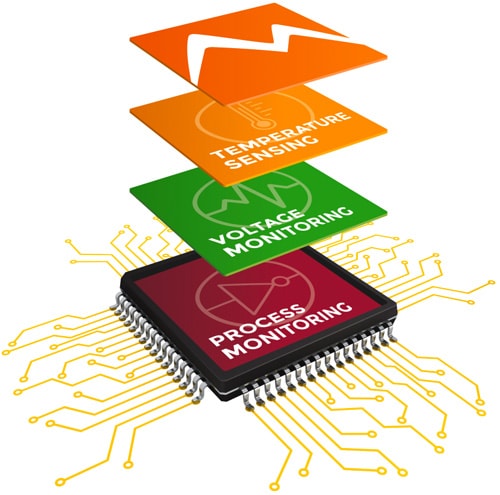
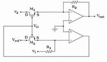
One holy grail of AI software developers is to create a system that is self-aware, or sentient. A less lofty goal than sentient AI is for chip designers to know how each specific chip responds to Process variations, Voltage levels and Temperature changes. If a design engineer knew exactly which process corner that each chip was fabricated… Read More
SEMI is a worldwide organization with local chapters like the one here in Oregon, where I attended a recent half-day presentation by several industry experts on the topic – Globalization, How it shapes the Semiconductor industry:
- Michael Chen, Director, Mentor – A Siemens Business
- John Brewer, CEO, Amorphyx
- Ed
…
Read More
I remember the days of the IDM (integrated device manufacturer). For me, it was RCA, where I worked for 15 years as the company changed from RCA to GE and then ultimately to Harris Semiconductor. It’s a bit of a cliché, but life was simpler then, from a customer point of view at least. RCA did it all. We designed all the IP, did the physical… Read More
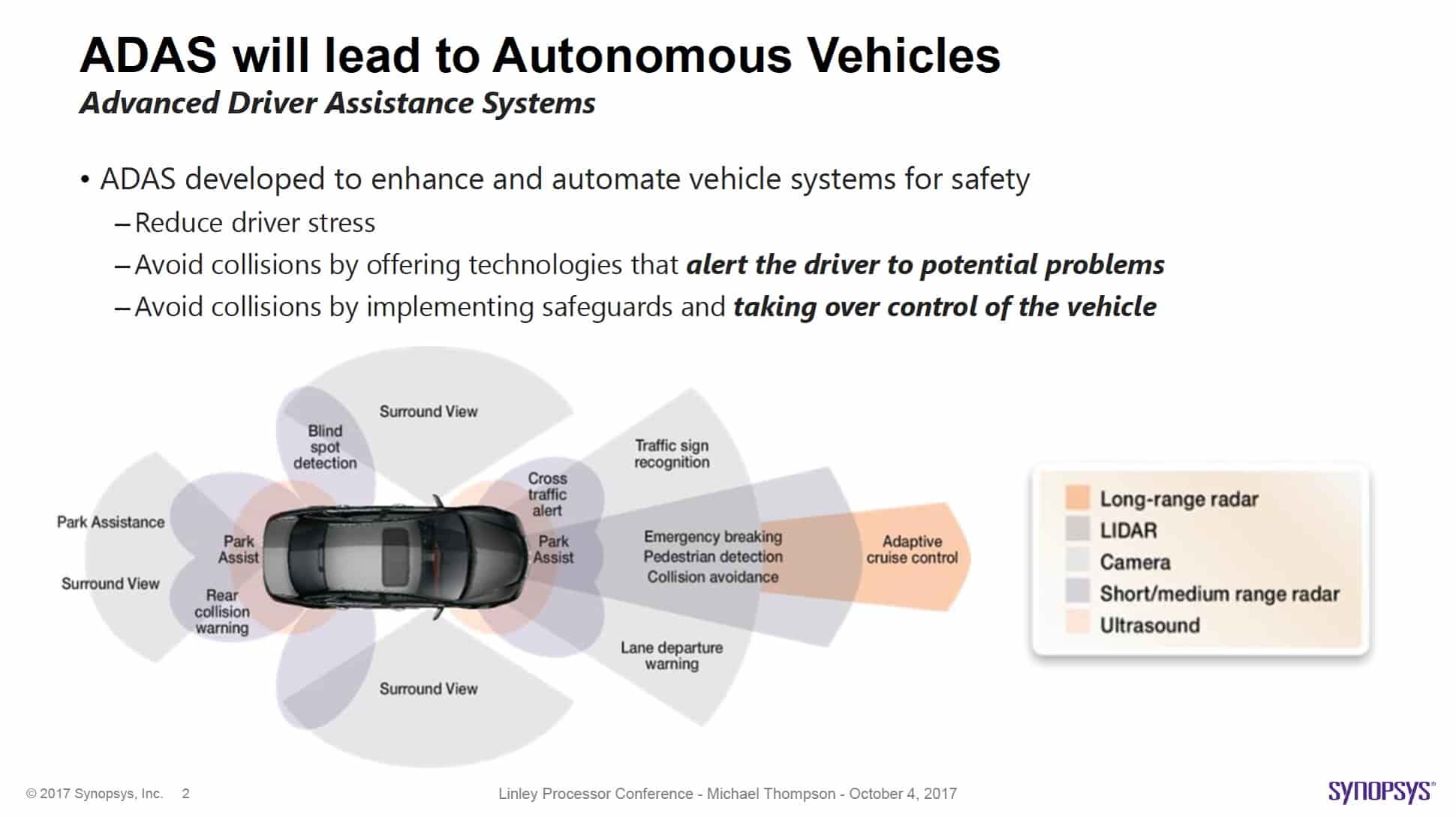
The reason you are seeing a lot more written about the ISO 26262 requirements for automotive electronics is, to put it bluntly, this stuff is getting real. Driver assist systems are no longer only found in the realm of Mercedes and Tesla, almost every car in every brand offers some driver assist features. However, the heavy lifting… Read More
Power integrity and reliability are just as important for AMS designs as they are for digital designs. Ansys is offering a series of five webinars on this topic, under a heading they call ANSYS in ACTION, a bi-weekly demo series from ANSYS in which an application engineer shows you how simulation can address common applications.… Read More
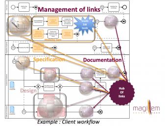
We have an urge to categorize companies, and when our limited perspective is of a company that helps with design, we categorize it as an EDA company. That was my view of Magillem, but I have commented before that my view is changing. I’m now more inclined to see them more as the design equivalent of a business intelligence organization… Read More
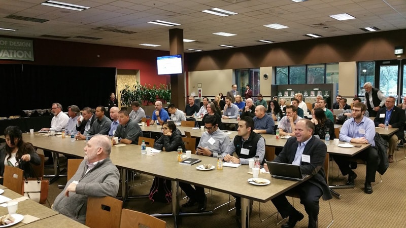
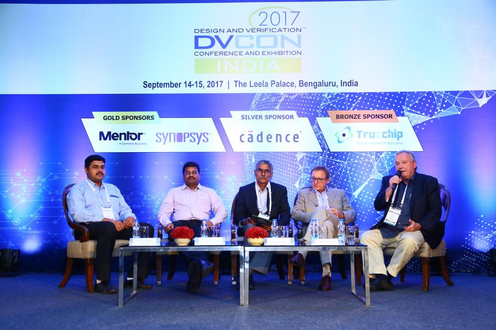
The fourth installment of DVCon India took place in Bangalore, September 14-15. As customary, it was hosted in the Leela Palace, a luxurious and tranquil resort in the center of Bangalore, and an excellent venue to host the popular event.
As reported in my previous DVCon India trip reports, the daily and evening traffic in Bangalore… Read More
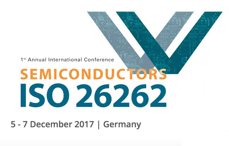
When we talk about the promise of ADAS and autonomous cars then along the way we also hear about this functional safety standard called ISO 26262 which semiconductor companies all pay close attention to. I recently learned about a new conference called Semiconductors ISO 26262, scheduled for December 5-7 in Munich, Germany. The… Read More
Despite all the enthusiastic discussion about security in the IoT and a healthy market in providers of solutions for the same, it is difficult to believe that we are doing more than falling further behind an accelerating problem. Simon Segars echoed this in his keynote speech at ARM TechCon this year. The issue may not be so much in… Read More
In life, there are some things that just go together. Imagine the world without peanut butter and jelly, eggs and potatoes, telephones and voicemail, or the internet and search engines. In the world of computing there are many such examples – UARTS and FIFO’s, processor cores and GPU’s, etc. Another trait all these things have is… Read More


Chemical Origins of Environmental Modifications to MOR Lithographic Chemistry