You are currently viewing SemiWiki as a guest which gives you limited access to the site. To view blog comments and experience other SemiWiki features you must be a registered member. Registration is fast, simple, and absolutely free so please,
join our community today!
WP_Term Object
(
    [term_id] => 157
    [name] => EDA
    [slug] => eda
    [term_group] => 0
    [term_taxonomy_id] => 157
    [taxonomy] => category
    [description] => Electronic Design Automation
    [parent] => 0
    [count] => 4517
    [filter] => raw
    [cat_ID] => 157
    [category_count] => 4517
    [category_description] => Electronic Design Automation
    [cat_name] => EDA
    [category_nicename] => eda
    [category_parent] => 0
    [is_post] =>
)
As is now traditional, Gary Smith kicked off DAC proper (there were workshops earlier and some co-located conferences started days before). He started by dismissing the idea that it costs $170M to do an SoC design.
In fact he looked at 3 different cases. Firstly, the completely unconstrained design. Well, no design is completely… Read More
This year’s Kaufman award winner is Chenming Hu. In contrast to previous years, this was presented on the Sunday evening of DAC instead of at a separate event in San Jose. Chenming’s career was reviewed by Klaus Schuegraf, Group Vice President of EUV Product Development at Cymer, Inc (now part of ASML) and also one of… Read More
Fractal Technologies is a privately held EDA company with offices in San Carlos, California and Eindhoven, the Netherlands. The company was founded by a small group of highly recognized EDA professionals. The scope of Fractal Technologies is to check consistency and validate all different data formats used in your design and… Read More
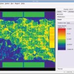
Thermal analysis has traditionally been given short shrift when compared to other more prominent issues facing chip designers. Invarian, to my eye at least, feels that the winds of change are in the air. Not that power or EM/IR issues will fade, that indeed is not the case and in fact quite the contrary, they are contributors to the… Read More
This list was compiled by the SemiWiki bloggers highlighting emerging technologies that we have written about and that will be demonstrated at the Design Automation Conference next week. We highly recommend you investigate them further during your time in Austin and please let us know what you think.
Today SemiWiki has more than… Read More
Robust Reliability Verification: Beyond Traditional Tools
by Matthew Hogan, Mentor Graphics
At all process nodes, countless hours are diligently expended to ensure that our integrated circuit (IC) designs will function in the way we intended, can be manufactured with satisfactory yields, and are delivered in a timely fashion… Read More
One of the other increasingly successful channels (besides Semiwiki of course) for EDA, IP and semiconductor companies to reach potential customers is John Cooley’s DeepChip. Every year he puts a lot of effort into trying to find out who is exhibiting what at DAC and which stuff seems like it is new and maybe important, and… Read More
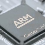
Just in time for DAC, Carbon have announced that they have expanded their partnership with ARM to create and deliver models for the ARM Cortex-A57 processor and related IP. One piece of related IP is the Cortex-A53 which can be configured in big.LITTLE multi-core setups to achieve the sweet spot of higher performance and lower power.… Read More
Auto makers have historically been accused of things like planned obsolescence – redesigning parts to make repairs painfully or even prohibitively expensive – and the “warranty time-bomb”, where major systems seem to fail about a week after the warranty expires. Optimists would chalk both those up to relentless innovation,… Read More
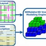
Yes, it’s a pleasant surprise; it is Virtual Fabrication Platform, one of the new innovations in 2013. I was looking around for what kind of breakthrough technologies will be announced in DAC this year. And here I came across this new kind of innovative tool which can produce final virtual fabricated 3D structures after following… Read More


Consolidation and Competition: Who is Winning the $4.5 Billion Interface IP Race?