You are currently viewing SemiWiki as a guest which gives you limited access to the site. To view blog comments and experience other SemiWiki features you must be a registered member. Registration is fast, simple, and absolutely free so please,
join our community today!
WP_Term Object
(
    [term_id] => 157
    [name] => EDA
    [slug] => eda
    [term_group] => 0
    [term_taxonomy_id] => 157
    [taxonomy] => category
    [description] => Electronic Design Automation
    [parent] => 0
    [count] => 4534
    [filter] => raw
    [cat_ID] => 157
    [category_count] => 4534
    [category_description] => Electronic Design Automation
    [cat_name] => EDA
    [category_nicename] => eda
    [category_parent] => 0
    [is_post] =>
)
During my illustrious career one of the most useful axioms that I use just about everyday day is: “Understand what people say but also understand why they are saying it.” This certainly applies to press releases so let’s take a look at what Intel unleashed during #51DAC (in alphabetical order):
ANSYS And Intel Collaborate… Read More
The ARC EM family is the low-power, embedded and low footprint processor part of the larger ARC processor. To target the ultra low-power markets like wearable and IoT, Synopsys has added DSP capabilities to EM5D and EM7D. To be specific, these cores are optimized for ultra low-power control and DSP, thanks to:
…
Read More
One of the benefits of spending the last 30 years working in Silicon Valley and publishing a fabless semiconductor book is that I get invitations to speak at events I would normally be attending. Being on the other side of the podium is truly a unique experience and one worth pursuing, absolutely. This month I spoke at #51DAC about … Read More
My favorite method to learn about EDA tools at DAC is by listening to actual IC designers, so on June 3rd I heard Jacob Bakker from NXP talk about his experience with noise coupled analysis for advanced mixed-signal automotive ICs.… Read More
In the semiconductor industry, it feels great to hear about the process technology shrinking to lower nodes along with innovative transistor structures that offer major gains in PPA (Power, Performance and Area). However, it requires huge investment of capital, time and effort from foundries to conceptualize, prototype and… Read More
Design Automation Conference Workshop on Suite of Embedded Applications and Kernels
In June, the first Suite of Embedded Applications and Kernels, or SEAK, workshop at the 2014 Design Automation Conference in San Francisco introduced a new Defense Advanced Research Projects Agency program in the area of embedded system benchmarking… Read More
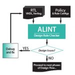
About a decade ago, semiconductor designs had just a few asynchronous clocks which were easily managed by designers through the process of manual design reviews. The situation today is completely different. An SoC can have hundreds of asynchronous clocks, driving different complex functions, spread across various IPs, supplied… Read More
Tools, tools, tools. Designs are rapidly changing, JESD204b, Hybrid Memory cube and all other Gigabit serialization schemes are here to stay. RIP DDR. This means board level simulations with respect to firmware (FPGA) are going to be more challenging than ever. Why? you ask, especially if the board layout is simpler? True, but… Read More
So first the one thing that you do know. MunEDA are based in Munich which makes them German. I have to confess that until I got involved helping them a bit with some marketing stuff that that was about all I knew about them too.
So now five things that you might not know:
1. MunEDA have a much wider customer list that you know and would even… Read More
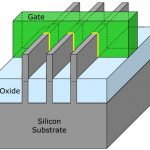
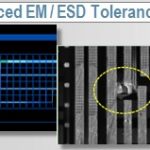
Although semiconductor manufacturing has taken off with FinFET based process technology which provides lucrative payoffs on performance improvement, power reduction and area saving in devices for high density and high performance SoC demand of modern era, apprehensions remain about its reliability due to reduced noise … Read More


Enhancing Multi-Domain System Simulation with FMI Co-Simulation