You are currently viewing SemiWiki as a guest which gives you limited access to the site. To view blog comments and experience other SemiWiki features you must be a registered member. Registration is fast, simple, and absolutely free so please,
join our community today!
WP_Term Object
(
    [term_id] => 157
    [name] => EDA
    [slug] => eda
    [term_group] => 0
    [term_taxonomy_id] => 157
    [taxonomy] => category
    [description] => Electronic Design Automation
    [parent] => 0
    [count] => 4440
    [filter] => raw
    [cat_ID] => 157
    [category_count] => 4440
    [category_description] => Electronic Design Automation
    [cat_name] => EDA
    [category_nicename] => eda
    [category_parent] => 0
    [is_post] =>
)
When it comes to wearable technology and the rapidly emerging world of IoT, sensors and MEMS are on the frontlines. They collect and transfer raw data such as pressure, temperature and motion and process it with algorithms critical to making sure the right information gets to humans and/or machines so the right reaction is enabled.… Read More
There is a data explosion:
- IBM says that 90% of all data was created in the last 2 years
- Smartphone processor development requires 100GB of data per engineer
- Android testing requires 30GB times the number of tests times the number of testers
- Biotech simulation, game development and more all require enormous amounts of data
This … Read More
On July 4, 2012, the European Organization for Nuclear Research, or CERN, announced that the ATLAS and CMS experiments had each observed a new particle, which is consistent with the Higgs boson predicted by the Standard Model of particle physics. The Compact Muon Solenoid (CMS) is a general-purpose detector with a broad physics… Read More
Does the evil sounding phenomenon known as Dark Silicon create a big opportunity for FPGA vendors as was predicted recently by Pacific Crest Securities? John Vinh posits that using multiple cores as a method of scaling throughput is flattening out, and the use of FPGA’s to perform computation can help off-load and thus overcome… Read More
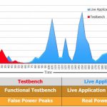
On your last SoC project how well did your dynamic power estimates match up with silicon results, especially while running real applications on your electronic product? If your answer was, “Well, not too good”, then keep reading this blog. A classical approach to dynamic power analysis is to run your functional testbench… Read More
In Chaucer’s Canterbury Tales, the second of the tales told by the pilgrims is The Miller’s Tale. Since this is a family blog, I’ll leave you to research the tale yourself. But FinFETs hide another Miller’s Tale, due to Miller capacitance, sometimes called the Miller effect. This is significant since in FinFET designs Miller capacitance… Read More
Synopsys had their earnings announcement and call last week. They were good. In Aart’s own words:I’m happy to report that our second quarter results were very strong and solidify our outlook for the full year. We delivered revenue of $557 million, non-GAAP earnings per share of $0.68 and $155 million in operation cash flow.… Read More
It’s very common these days to hear about a billion gates SoC, but not without a huge design and verification effort and investment of resources. A complete verification of such an SoC needs several verification steps including software and hardware based methodologies that often are not sufficient to cover the whole SoC. In order… Read More
One task that is not very exciting but is critical is that of library quality assurance. Many design groups have created their own procedures, often having been burned in the past, to ensure that the libraries that they use are good. Failure to do so has resulted in:… Read More
Silicon Photonics is the hottest prospect for blazing fast communication between chips in servers, data centers, and supercomputers.
By using light instead of electrical signals, it promise to usher in a new standard of high performance, low power devices while extending the use of more mature process nodes, helping to reduce… Read More


Silicon Insurance: Why eFPGA is Cheaper Than a Respin — and Why It Matters in the Intel 18A Era