NVIDIA has been teasing the promise of Pascal for years, but this year Pascal’s performance became much more real. With the announcement of the Tesla P100 based on Pascal, NVIDIA was able to show the neural-network world what Pascal was really capable of. However, that chip is very different from the gaming-focused Pascal chip … Read More

Electronic Design Automation
OpenPOWER Keeps On Truckin’ At Annual Development Summit
The OpenPOWER Foundation, a collection of companies that have coalesced around IBM’s POWER architecture recently had their OpenPOWER Summit in San Jose, California. OpenPOWER was founded by IBM, Google, Tyan and Mellanox to coalesce around IBM’s approach towards opening up the POWER architecture to anyone that wishes to license… Read More
Free Webinar: Designing Low-Power IoT Systems

As I have written before, IoT looks to be a key driver for design starts and future semiconductor revenue growth which is why we wrote “PROTOTYPICAL” and included a field guide to FPGA Prototyping. If you want to get funding for your new IoT chip project, having a working prototype is a good thing, absolutely. If you want to take a look… Read More
Reusable HW/SW Interface for Portable Stimulus
Although semiconductor community has ushered into the era of SoCs, the verification of SoCs is still broken. There is no single methodology or engine to verify a complete SoC; this results in duplication of efforts and resources for test creation and verification at multiple stages in the SoC development, albeit with different… Read More
iDRM – A Complete Design Rule Development System

Design rules are at the heart of the interface between the foundry and semiconductor designers, which makes them so critical. Traditionally, design rules and DRC decks have been developed manually with no or little automation. Design rule definitions are written using WORD or other general purpose office tools, and DRC decks… Read More
Quick Guide to FD-SOI at #53DAC
If you’re headed to #53DAC (June 5-9 in Austin,TX) and are interested in learning more about FD-SOI, there will be lots of opportunities. Here’s a quick guide to get you started. … Read More
Layout Pattern Matching for DRC, DFM, and Yield Improvement
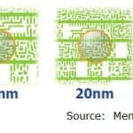
It is truly amazing to consider the advances in microelectronic process development, using 193i photolithography. The figure below is a stark reminder of the difference between the illuminating wavelength and the final imaged geometries. This technology evolution has been enabled by continued investment in mask data generation… Read More
Go Native – With Methodics at DAC in Austin

DAC is often a yearly reflection point for the companies that exhibit and attend. For the innovators it is an opportunity to look back and see a year of progress and development. Fortunately, this is the case for Methodics, which has had a strong year both in terms of business and technical development. Though, we easily see how these… Read More
Why USB 3.1 Certification is a “Must Have”?
USB 3 protocol is now height years old, but USB 3.1 is much more recent (2014). The adoption behavior for USB protocol is unique, as USB 2.0 bandwidth (480 Mbps) is largely enough for certain applications. Nevertheless we have seen the sales for USB 3 IP passing the USB 2 in value during 2014, and the total USB IP segment becoming the … Read More
Musk’s Orbital Compute Vision: TERAFAB and the End of the Terrestrial Data Center