You are currently viewing SemiWiki as a guest which gives you limited access to the site. To view blog comments and experience other SemiWiki features you must be a registered member. Registration is fast, simple, and absolutely free so please,
join our community today!
WP_Term Object
(
    [term_id] => 157
    [name] => EDA
    [slug] => eda
    [term_group] => 0
    [term_taxonomy_id] => 157
    [taxonomy] => category
    [description] => Electronic Design Automation
    [parent] => 0
    [count] => 4441
    [filter] => raw
    [cat_ID] => 157
    [category_count] => 4441
    [category_description] => Electronic Design Automation
    [cat_name] => EDA
    [category_nicename] => eda
    [category_parent] => 0
    [is_post] =>
)
High Level Synthesis Updateby Tom Dillinger on 06-29-2016 at 7:00 amCategories: EDA, Siemens EDA
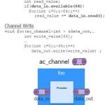
High-level synthesis (HLS) involves the generation of an RTL hardware model from a C/C++/SystemC description. The C code is typically referred to as abehavioraloralgorithmicmodel. The C language constructs and semantics available to architects enable efficient and concise coding – the code itself is smaller, easier to write/read,… Read More
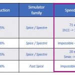
Spice circuit simulation remains the backbone of IC design validation. Digital cell library developers rely upon Spice for circuit characterization, to provide the data for Liberty models. Memory IP designers utilize additional Spice features to perform statistical sampling. Analog and I/O interface designers extend these… Read More
Most mergers and acquisitions in the EDA world simply don’t work out financially a year or two after the deal is done, however I was pleasantly surprised to learn that Tanner EDA is doing quite well at #53DAC this year after the acquisition by Mentor Graphics back in March 2015. Everyone that I’ve been meeting with at … Read More
Every day I read stuff about the coming of fully autonomous vehicles, and it’s not every day we get a technologist’s view of the hurdles faced in getting there. Chris Rowen, CTO of Cadence’s IP group, gave one of the best presentations I’ve seen on ADAS technology and convolutional neural networks (CNNs) at #53DAC, pointing… Read More
Charlene Marini (VP of ARM Segment Marketing) did a nice presentation at the ARM/Mentor Summit last month at the Mentor HQ in Fremont. I just got the slides so let me give you a quick summary from my notes. It was a very good presentation on IoT and emulation which in my mind is the new simulation. I also attended an IoT panel at #53DAC that… Read More
In our semiconductor ecosystem we often specialize the engineers and therefore EDA tools into separate silos like Foundry, front-end design, back-end design, tapeout, etc. What I discovered at #53DAC a few weeks ago was that some EDA companies actually bridge the gap between foundry engineers and IC designers with their tools.… Read More
At NVIDIA’s GPU Technology Conference (GTC) 2016 in San Jose, California the company announced products based on their latest GPU architecture, code-named Pascal. This conference is traditionally attended by some of the leading researchers in GPU-accelerated compute technologies and over the past few years has become increasingly… Read More
At the #53DAC earlier this month held in Austin, Texas I met up with Renee Donkers, the founder of Fractal Technologies. His company has been focused on improving the quality of semiconductor IP cells through the use of automated checking software. The highest area of growth in EDA as measured by the ESD Alliance is in the reusable… Read More
In case you worry that IBM will abandon hardware in the pursuit of its strategic initiatives focusing on cloud, mobile, analytics and more; well, stop worrying. With the announcement of its POWER Roadmap at the OpenPOWER Summitearlier this spring, it appears POWER will be around for years to come. But IBM is not abandoning the strategic… Read More
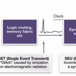
We’ve introduced the concepts behind triple modular redundancy (TMR) before, using built-in capability in Synopsys Synplify Premier to synthesize TMR circuitry into FPGAs automatically. A recent white paper authored by Angela Sutton revisits the subject… Read More


Musk’s Orbital Compute Vision: TERAFAB and the End of the Terrestrial Data Center