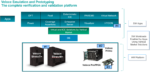
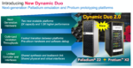
SILVACO 073125 Webinar 800x100
WP_Term Object
(
    [term_id] => 157
    [name] => EDA
    [slug] => eda
    [term_group] => 0
    [term_taxonomy_id] => 157
    [taxonomy] => category
    [description] => Electronic Design Automation
    [parent] => 0
    [count] => 4182
    [filter] => raw
    [cat_ID] => 157
    [category_count] => 4182
    [category_description] => Electronic Design Automation
    [cat_name] => EDA
    [category_nicename] => eda
    [category_parent] => 0
    [is_post] => 
)

Cadence Digital Full Flow Optimized to Deliver Improved Quality of Results with Up to 3X Faster Throughput

Cadence Digital Full Flow Optimized to Deliver Improved Quality of Results with Up to 3X Faster Throughput
by Mike Gianfagna on 03-23-2020 at 6:00 am

FINAL2 Digital FF iSpatial Flow hi res

Artificial intelligence (AI) and machine learning (ML) are hot topics. Beyond the impact these technologies are having on the world around us, they are also having impact on the semiconductor and EDA ecosystem. I posted a blog last week that discussed how Cadence views AI/ML, both from a tool and ecosystem perspective. The is one… Read More


A Conversation with Wally Rhines: Predicting Semiconductor Business Trends After Moore’s Law

A Conversation with Wally Rhines: Predicting Semiconductor Business Trends After Moore’s Law
by Daniel Nenni on 03-22-2020 at 10:00 am

Cover Predicting Trends

Wally Rhines is one of the most prolific speakers the semiconductor industry has ever experienced. Wally is also one of the most read bloggers on SemiWiki.com, sharing his life’s story which is captured in his first book: From Wild West to Modern Life the Semiconductor Evolution.

On April 2nd at 10am PDT we will host Wally on a live… Read More


Machine Learning for EDA – Inside, Outside and Everywhere Else

Machine Learning for EDA – Inside, Outside and Everywhere Else
by Mike Gianfagna on 03-18-2020 at 6:00 am

Paul Cunningham

Artificial intelligence (AI) is everywhere. The rise of the machines is upon us in case you haven’t noticed. Machine learning (ML) and its associated inference abilities promise to revolutionize everything from driving your car to making breakfast. We hear a lot about the macro, end-product impact of this technology, but there… Read More


Webinar on Tools and Solutions for Analog IP Migration

Webinar on Tools and Solutions for Analog IP Migration
by Tom Simon on 03-17-2020 at 10:00 am

MunEDA flow for analog design porting

The commonly advanced reason for IP reuse is lower cost and shorter development time. However, IP reuse presents its own challenges, especially for analog designs. In the case of digital designs, once a new standard cell library is available, it is usually not too hard to resynthesize RTL to create new working silicon. For analog… Read More


Innovation in Verification March 2020

Innovation in Verification March 2020
by Bernard Murphy on 03-17-2020 at 6:00 am

Innovation

This blog is the next in a series in which Paul Cunningham (GM of the Verification Group at Cadence), Jim Hogan and I pick a paper on a novel idea we appreciated and suggest opportunities to further build on that idea.

We welcome comments on our blogs and suggestions for new topics if they’re based on published work.

The Innovation

Our… Read More


5G SoCs Demand New Verification Approaches

5G SoCs Demand New Verification Approaches
by Mike Gianfagna on 03-16-2020 at 10:00 am

Simplified 4G network

Lately, I’ve been cataloging the number of impossible-to-verify technologies we face. All forms of machine learning and inference applications fall into this category. I’ve yet to see a regression test to prove a chip for an autonomous driving system will do the right thing in all cases. Training data bias is another interesting… Read More


Why IP Designers Don’t Like Surprises!

Why IP Designers Don’t Like Surprises!
by Daniel Nenni on 03-13-2020 at 6:00 am

IPDelta SemiWiki

If it’s your job to get a SoC design through synthesis, timing/power closure and final verification, the last thing you need are surprises in new versions of the IP blocks that are integrated into the design. If your IP supplier sends a new version, the best possible scenario is that this is only a small incremental change from… Read More


Viewing the Largest IC Layout Files Quickly

Viewing the Largest IC Layout Files Quickly
by Daniel Payne on 03-10-2020 at 6:00 am

Skipper, Empyrean

The old adage, “Time is money”, certainly rings true today for IC designers, so the entire EDA industry has focused on this challenging goal of making tools that help speed up design and physical verification tasks like DRC (Design Rule Checks) and LVS (Layout Versus Schematic). Sure, the big three EDA vendors have… Read More


Achieving Design Robustness in Signoff for Advanced Node Digital Designs

Achieving Design Robustness in Signoff for Advanced Node Digital Designs
by Mike Gianfagna on 03-09-2020 at 10:00 am

Synopsys SemiWiki STARRC Webinar 1

I had the opportunity to preview an upcoming webinar on SemiWiki that deals with design robustness for signoff regarding advanced node digital designs (think single-digit nanometers). “Design robustness” is a key term – it refers to high quality, high yielding SoCs that come up quickly and reliably in the target system. We all… Read More


Six Automated Steps to Design Partitioning for Multi-FPGA Prototyping Boards

Six Automated Steps to Design Partitioning for Multi-FPGA Prototyping Boards
by Daniel Nenni on 03-09-2020 at 6:00 am

Aldec Webinar SemiWiki

Before starting your next FPGA Prototyping Project you should catch the next SemiWiki webinar – “Six Automated Steps to Design Partitioning for Multi-FPGA Prototyping Boards”, in partnership with Aldec.

A significant portion of my  30+ years in the EDA industry has revolved around design verification with some form of FPGA … Read More