
Predictions in technology adoption often hinge on a delicate balance between technical feasibility and market dynamics. While business considerations play a pivotal role, the technical category reasons for the success or failure of a prediction are more tangible and often easier to identify—if scrutinized with care. However,… Read More
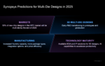
Will 50% of New High Performance Computing (HPC) Chip Designs be Multi-Die in 2025?


Captain America: Can Elon Musk Save America’s Chip Manufacturing Industry?