You are currently viewing SemiWiki as a guest which gives you limited access to the site. To view blog comments and experience other SemiWiki features you must be a registered member. Registration is fast, simple, and absolutely free so please,
join our community today!
The design of parallel interfaces is supposed to be (comparatively) easy — e.g., follow a few printed circuit board routing guidelines; pay attention to data/clock/strobe signal lengths and shielding; ensure good current return paths (avoid discontinuities); match the terminating resistances to the PCB trace impedance;… Read More
I recently had the opportunity to chat with Anirudh Devgan, senior vice president and general manager at Cadence, who leads the Digital and Signoff Group. We discussed recent product development initiatives at Cadence, and talked about future EDA and semiconductor market opportunities. His insights and comments were keen … Read More
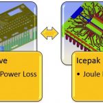
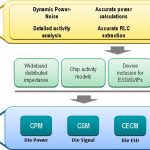
2015 will be remembered as the year when chip-package-system (CPS) physical co-design and electrical/thermal analysis methodologies took center stage.… Read More
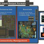
A new term has entered the vernacular of electronic design engineering — pathfinding. The complexity of the functionality to be integrated and the myriad of chip, package, and board technologies available make the implementation decision a daunting task. Pathfinding refers to the method by which the design space of technology… Read More
Expanding 3D EM Simulation Access to Allby Tom Dillinger on 02-03-2016 at 7:00 amCategories: Cadence, EDA
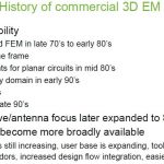
James Clerk Maxwell’s eponymous equations are the basis for simulating electromagnetic wave propagation. In school, EE majors tended to fall into two camps: (a) those that thoroughly enjoyed their fields and waves classes, who liked doing surface integrals, and who were adept at demonstrating the “right hand rule”, and (b) … Read More
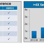
HSPICE – 35 and looking good!by Tom Dillinger on 02-01-2016 at 12:00 pmCategories: EDA, Synopsys
A maturetool. A legacytool. A tool that’s a little long in the tooth. We have all used these terms to refer to an EDA product that has not been able to keep up with technical challenges of model complexity, performance, or new features required by current SoC and system design requirements.… Read More
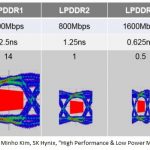
DesignCon is a unique conference — its tagline is “Where the Chip meets the Board”. Held each January in Santa Clara, the conference showcases a wealth of new technologies for advanced packaging, printed circuit board fabrication, connectors, cables, and related analysis equipment (e.g, BERT, VNA, scopes). Of specific… Read More
The 50 year anniversary of the publication of Moore’s Law was recently celebrated, highlighting the tremendous advances in the Microelectronics Eraof the period in human history known as the Information Age. However, the technical and economic challenges currently faced by the microelectronics industry are bringing into… Read More
Looking back, 2015 was a significant year for mergers and acquisitions in the EDA industry. The Semiwiki team maintains a chronology of major transactions here.
As I was reviewing this compendium, one of the entries that stands out is the acquisition of Apache Design Solutions by Ansys, Inc. a couple of years ago.
At that time, there… Read More
The most exciting products in our industry are those that are both evolutionary and revolutionary. Cadence has just announced an update to their hardware simulation acceleration platform – Palladium Z1 – which continues the evolution of the unique capabilities of processor-based acceleration, plus a revolutionary approach… Read More


TSMC CoWoS versus Intel EMIB Semiconductor Packaging